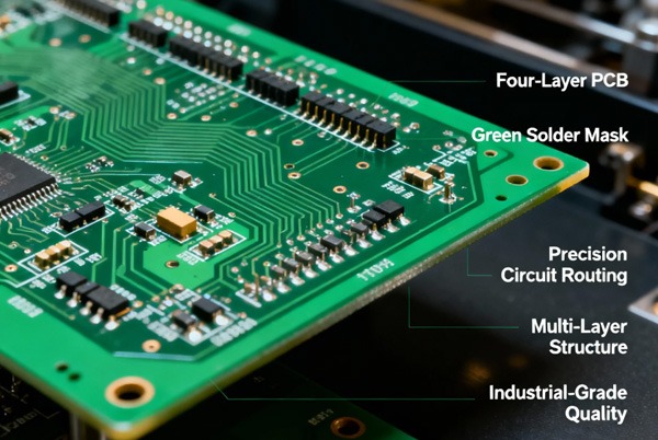
In consumer electronics, industrial control equipment, and high-speed digital systems, four-layer PCBs are widely favored for their superior electromagnetic compatibility (EMC), power integrity, and signal integrity.
Table of Contents
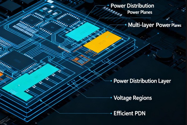
4-Layer PCB Stackup Structure
The stackup design is the foundation of a 4-layer board’s performance. An improper stackup can lead to signal crosstalk, power supply noise, and EMI non-compliance.
1. Comparison of Classic Stackup Schemes
- Scheme 1 (Recommended)
- Top Layer: Signal Layer
- Layer 2: Ground Plane (GND)
- Layer 3: Power Plane (PWR)
- Bottom Layer: Signal Layer
- Advantages: The ground plane provides a solid reference for top-layer signals. The adjacent power and ground planes form inherent decoupling capacitance.
- Scheme 2
- Top Layer: Signal Layer
- Layer 2: Power Plane
- Layer 3: Ground Plane
- Bottom Layer: Signal Layer
- Applicable Scenarios: High-current devices (e.g., motor drivers). Note potential reference plane changes for bottom-layer signals.
- Scheme 3 (Use with Caution)
- Top Layer: Ground Plane
- Layer 2: Signal Layer
- Layer 3: Signal Layer
- Bottom Layer: Power Plane
- Risks: Incomplete ground plane, long signal return paths. Suitable primarily for low-frequency, connector-dominated boards.
2. Key Parameter Settings
- Dielectric Thickness: Recommended 0.1–0.2mm between signal and reference planes to enhance inter-layer coupling.
- Copper Weight: Outer layers 1oz (35μm), inner layers 0.5oz (17.5μm). Can increase to 2oz for high-current areas.
- Pullback Design: Power planes should be indented 40–80mil relative to the ground plane (20H rule) to reduce edge radiation.
Via Design
Vias are crucial for inter-layer connections but introduce parasitic parameters affecting high-speed signals.
1. Via Type Selection
- Through-Hole Vias: Low cost, suitable for standard signals and power connections.
- Blind/Buried Vias: Used for high-density BGA escape routing, but increase process cost.
2. Parasitic Parameter Calculation
- Parasitic Capacitance:
C ≈ 1.41ε · T · D1 / (D2 - D1)
WhereTis board thickness,D1is drill diameter,D2is the pad diameter. - Parasitic Inductance:
L ≈ 5.08h [ln(4h / d) + 1]
Wherehis via length,dis drill diameter.
3. Via Usage Guidelines
- Power Vias: Use larger vias (e.g., 12mil diameter/16mil drill), place multiple in parallel to reduce impedance.
- Signal Vias: Prefer smaller vias (e.g., 8mil diameter/12mil drill). Avoid asymmetric placement in differential pairs.
- Thermal Vias: Place under heat-generating components (e.g., 0.3mm drill, 1.5mm pitch).
PCB Routing
1. Routing Procedure
- Tackle Difficult Areas First: Start routing from complex areas like BGAs and high-speed interfaces.
- Modular Handling: Route by functional blocks (e.g., MCU, memory, analog circuits) to prevent cross-interference.
- Clean-up Routing: Route low-speed signals last, optimizing channel utilization by adjusting trace width and spacing.
2. Critical Routing Rules
- Impedance Control:
- Single-ended: 50Ω. Differential pairs: 100Ω.
- Achieve by adjusting trace width, dielectric thickness, and permittivity.
- High-Speed Signal Handling:
- Prioritize routing clock signals on inner layers, referenced to a ground plane.
- Maintain length matching in differential pairs (≤5mil tolerance).
- Power Plane Segmentation:
- Segment a single power plane into a maximum of 3 regions (e.g., 3.3V, 5V, 12V).
- Use segmentation lines ≥0.5mm wide to prevent creepage issues.
Power Integrity Design
1. Decoupling Capacitor Placement
- Selection: 0.1μF ceramic capacitors (high-frequency) + 10μF tantalum capacitors (low-frequency).
- Placement: Position close to IC power pins (≤3mm). Connect directly to power/ground planes via vias.
2. Ground Plane Integrity
- Avoid splitting the ground plane with signal traces to ensure low-impedance return paths.
- Connect digital and analog grounds at a single point using a ferrite bead or 0Ω resistor.
Design Verification & Production Preparation
1. DRC Checklist
- Trace Width/Spacing: General signals ≥6/6mil, Power traces ≥12/12mil.
- Drill-to-Copper Distance: ≥8mil to prevent short circuits.
2. Signal Integrity Simulation
- Use tools like HyperLynx or Sigrity to check rise time, ringing, and impedance continuity.
- Focus on verifying clocks, differential signals, and power supply ripple.
3. Production File Output
- Provide Gerber files (includes layers, solder mask, drill), impedance test coupons, and assembly drawings.
Key Design Takeaways
- Prefer Stackup Scheme 1, ensuring a ground plane adjacent to primary signal layers.
- Balance cost and performance via design, using parallel power vias to reduce impedance.
- Route following the “Difficult First” principle, prioritizing high-speed signals on inner layers.
- Limit power segmentation to 3 regions, placing decoupling capacitors close to ICs.
- Validate with both DRC and simulation to avoid post-production rework.