Under the trend of high-speed and miniaturization of modern electronic equipment, multilayer PCB design is facing unprecedented challenges. In this paper, we will discuss the key technology of blind vias, from the basic principles to practical applications, to reveal how to solve the signal integrity problems in high-speed design through blind vias.
Table of Contents
PCB Drilling Technology Overview
Mechanical Drilling: Traditional Yet Indispensable
- Suitable hole diameter: Typically above 0.15mm
- Drill bit material: Tungsten steel or diamond-coated
- Cost advantage: Extremely low unit price for mass production
- Limitations: Difficulty in microvia processing, minimum hole size restrictions
Laser Drilling: The Preferred Choice for High Precision
- CO2 laser: Suitable for 50-150μm hole diameters, fast processing speed
- UV laser: Can process 20-50μm ultra-micro vias with higher precision
- Characteristics: Non-contact processing, no mechanical stress
Special Drilling Technologies
- Plasma drilling: Used for flexible boards and special materials
- Water jet drilling: No heat-affected zone, suitable for sensitive materials
- Mechanical-laser composite drilling: Combines the advantages of both for thick board processing
In-depth analysis of the blind hole process
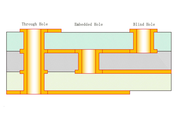
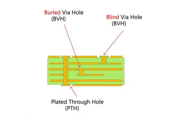
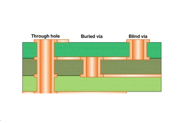
What is a blind hole?
Blind vias are vias that extend from the surface of the PCB to an internal layer only and do not run through the entire board, like a “zone elevator” in a tall building that stops at a specific floor instead of going to all floors. This selective connectivity revolutionizes high-speed design.
Blind Via vs Through-Hole: Performance Comparison
| Metric | Blind Via | Through-Hole |
|---|---|---|
| Signal path length | 30-70% shorter | Full penetration |
| Crosstalk level | 40-60% lower | Relatively high |
| Wiring density | 2-3 times higher | Basic level |
| Manufacturing cost | 20-50% higher | Baseline cost |
Core Benefits of the Blind Vias Process
Signal Integrity Improvement: Blind vias significantly shorten the signal transmission path, reducing signal reflections and losses. Studies have shown that signal reflections can be reduced by more than 40% with blind vias.
Improved EMC: By eliminating unnecessary through-hole penetrations, blind vias effectively reduce electromagnetic interference (EMI) and signal crosstalk, which is especially critical in high-frequency applications in the GHz class.
Increased Design Freedom: Blind vias free up valuable wiring space, allowing engineers to realize more complex interconnect designs in a smaller area.
Product miniaturization boost: Compared to through-hole designs, the blind vias process saves up to 30% of board space, providing the technical basis for slimming down modern electronic devices.
Detailed Explanation of Blind Via Manufacturing Process
1. Precision Alignment Stage
- Laser positioning system: Uses CCD visual alignment with ±5μm accuracy
- Shrinkage compensation: Pre-compensates 0.05-0.1% based on material properties
- Reference marks: Designs 3-5 global alignment targets
2. Key Controls in Laser Drilling
- Energy control: Uses pulsed energy gradient adjustment technology
- Focus management: Dynamic Z-axis focusing ensures interlayer consistency
- Dust removal system: Real-time suction prevents residue redeposition
Typical Parameter Examples:
- UV laser: 355nm wavelength, 20ns pulse width
- For 100μm diameter: Single hole processing time ≈3ms
- Repositioning accuracy: ±3μm
3. Via Wall Treatment Process
- Plasma cleaning:
- Gas mixture: O₂(80%)+CF₄(20%)
- Power: 300-500W
- Duration: 45-90 seconds
- Chemical micro-etching:
- Sulfuric acid-hydrogen peroxide system
- Controls copper surface roughness at 0.2-0.5μm
4. Key Metallization Steps
- Electroless copper plating:
- Thickness: 0.3-0.8μm
- Deposition rate: 2-4μm/h
- Electroplating thickening:
- Uses pulse plating technology
- Target thickness: 15-25μm
- Uniformity control: ≤10%
5. Pattern Transfer Optimization
- Laser Direct Imaging (LDI):
- Resolution: 10μm line width/spacing
- Alignment accuracy: ±8μm
- Dry film lamination:
- Pressure: 0.4-0.6MPa
- Temperature: 100-110℃
Solutions to Five Common Practical Problems
Q1: How to prevent resin depression at blind via locations?
A: Resin depression is typically caused by excessive drilling energy or heat-sensitive materials. Recommendations:
- Optimize laser parameters: Reduce single pulse energy, increase pulse count
- Switch to high-Tg materials: e.g., Isola 370HR (Tg=180℃)
- Post-processing: Use via filling plating or conductive adhesive filling
Q2: How to solve impedance discontinuity when high-frequency signals pass through blind vias?
A: Solutions for impedance discontinuity:
- Design compensation: Add antipads at via necks
- Structural optimization: Use tapered blind vias (larger top, smaller bottom)
- Material selection: Use low-Dk variation materials (e.g., Rogers RO4835)
- Simulation verification: Optimize with HFSS or CST beforehand
Q3: How to address significant yield fluctuations in blind via mass production?
A: Stabilizing yield requires systematic control:
- Equipment maintenance: Daily laser optical path calibration
- Parameter monitoring: Real-time recording of key parameters (energy, focus, etc.)
- First-article inspection: Cross-section analysis for each batch
- SPC control: Establish control charts for key parameters (e.g., via diameter CPK>1.33)
Q4: How to resolve interlayer misalignment in HDI boards with stacked blind and buried vias?
A: Solutions for multilayer stacked via alignment:
- Material matching: Select low-shrinkage materials (e.g., MEGTRON6)
- Process optimization: Use sequential lamination technology
- Alignment design: Add optical alignment targets
- Compensation algorithm: Dynamic compensation based on previous lamination shrinkage data
Q5: How to reduce manufacturing costs for blind vias in 8+ layer PCBs?
A: Cost control strategies for high-layer-count boards:
- Design optimization: Reduce unnecessary blind vias
- Process combination: Use blind vias for critical signal layers, through-holes for others
- Batch consolidation: Share production panels with other orders
- Manufacturer collaboration: Involve PCB fabricators early in design reviews
Advanced Process Techniques
Golden Rules for Laser Drilling Parameters
- Copper layer drilling: High energy + short pulse (e.g., 1mJ/10ns)
- Dielectric layer drilling: Low energy + long pulse (e.g., 0.5mJ/20ns)
- Mixed materials: Use energy gradient algorithms
Special Blind Via Treatment Techniques
- Copper-capped blind vias: Surface copper bumps enhance solder reliability
- Filled blind vias: Electroplated copper filling improves thermal conduction
- Stepped blind vias: Combined different layer depths optimize space utilization
Key Reliability Verification Points
- Thermal stress testing: -55℃~125℃ cycling for 1000 cycles
- IST testing: Current stress testing for 500 cycles
- Cross-section analysis: Inspect via wall copper thickness uniformity
- Impedance testing: TDR measurement for impedance consistency (±10%)
In-Depth Case Studies of Industry Applications
Case 1: 5G Millimeter-Wave Antenna Module
- Challenge: 77GHz signal transmission loss requirement <0.3dB/inch
- Solution:
- Adopted a 1-2 layer tapered blind via design
- Used Rogers RO3003 material
- Added plasma treatment after laser drilling
- Results: 42% reduction in insertion loss, 15% improvement in antenna efficiency
Case 2: High-Performance Computing GPU
- Challenge: Implementing 0.4mm BGA escape routing on a 16-layer PCB
- Innovations:
- 1-3-5 layer stepped blind via design
- Combined laser direct drilling with mechanical drilling
- Via filling plating for planarization
- Outcomes: 60% increase in routing channels, achieved 32Gbps signal rate
Future Technology Frontiers
Photon Drilling Technology:
- Femtosecond laser applications: Reduce heat-affected zones
- Intelligent drilling path planning: AI-optimized processing sequence
- Online inspection systems: 3D topography measurement during processing
Material Innovation Directions:
- Low-loss laser-processable dielectric materials
- Nano-composite copper paste via filling technology
- Self-assembled molecular layer via wall treatment