Multilayer PCBs (Printed Circuit Boards) are a sophisticated evolution of traditional single-sided and double-sided PCBs. These advanced circuit boards consist of multiple layers of conductive material, separated by insulating layers (dielectrics), all interconnected to create complex electronic circuits. Multilayer PCBs offer several significant advantages compared to their simpler counterparts, making them integral to modern electronics.
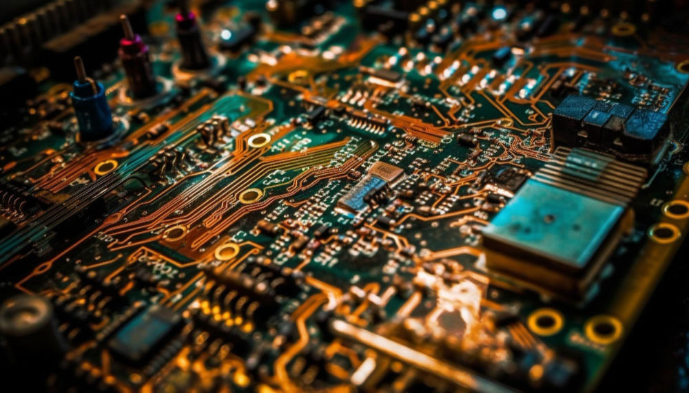
Table of Contents
Features of Multilayer PCBs
- Increased Density: Multilayer PCBs allow for a higher density of components and traces in a smaller space, enabling more functionalities in compact devices. This is especially valuable for today’s miniaturized electronics.
- Improved Signal Integrity: The multiple layers in these PCBs provide dedicated ground and power planes, which reduce electromagnetic interference and ensure better signal integrity, especially in high-frequency applications.
- Enhanced Performance: The dedicated power and ground planes also aid in efficient heat dissipation, which is crucial for maintaining the performance and reliability of high-power electronic devices.
- Reduced Noise: Multilayer PCBs effectively minimize crosstalk between traces and reduce noise, contributing to better overall circuit performance.
- Complex Designs: With multiple layers, designers can create intricate and complex circuit designs, incorporating advanced features like differential pairs, impedance-controlled traces, and high-speed data channels.
- Flexible Routing: The additional layers enable more routing options and easier integration of various components, leading to efficient use of space and improved design aesthetics.
- Integration of Components: Multilayer PCBs can accommodate surface-mount components on both sides, further enhancing their compactness and component density.
- Miniaturization: Multilayer PCBs are indispensable for modern devices where miniaturization is a key factor, such as smartphones, wearables, medical devices, and IoT gadgets.
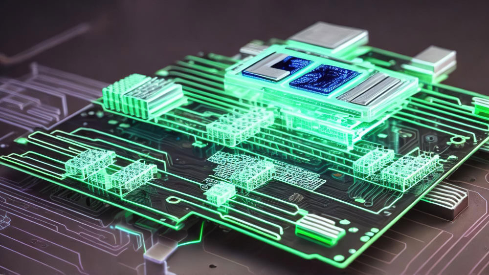
- Layer Stacking: These PCBs can have multiple layers, typically ranging from four to tens of layers, with each layer contributing to the overall functionality and performance of the circuit.
- Manufacturing Complexity: Designing and manufacturing multilayer PCBs require advanced software tools and specialized techniques. The process includes laminating layers together and ensuring accurate registration of the circuit patterns.

While multilayer PCBs offer numerous benefits, their complexity does make them more challenging to design and manufacture compared to single-sided or double-sided PCBs. Proper design, stack-up planning, and signal integrity analysis are critical to achieving optimal performance. Therefore, collaborating with experienced PCB manufacturers and designers is essential when dealing with multilayer PCB projects. Overall, multilayer PCBs play a pivotal role in driving innovation and pushing the boundaries of electronic design in the modern world.
Understand the Difference Between Multilayer, High Frequency and High Speed PCBs
Multilayer PCBs, high-frequency PCBs and high speed PCBs are tree distinct categories of printed circuit boards, each tailored to specific technological requirements. While both types share some characteristics, they serve different purposes and come with unique design considerations.
Multilayer PCBs
Multilayer PCBs consist of multiple layers of conductive material separated by insulating dielectric layers. They are designed to accommodate a higher density of components and traces in a compact form factor. The additional layers provide advantages such as reduced noise, improved heat dissipation, and enhanced signal integrity. Multilayer PCBs are commonly used in a wide range of applications, from consumer electronics to industrial equipment, where complex circuitry and efficient use of space are crucial. The primary focus of multilayer PCBs is on achieving compactness, optimal routing, and overall functionality, rather than targeting specific frequency ranges.
High-Frequency PCBs
High-frequency PCBs, on the other hand, are specialized boards designed to handle radio frequency (RF) and microwave signals with minimal loss and signal degradation. These PCBs are engineered to maintain consistent impedance, reduce electromagnetic interference, and ensure accurate signal propagation across a broad frequency spectrum. High-frequency PCBs require careful design techniques such as controlled impedance routing, transmission line optimization, and proper grounding to maintain signal integrity. They are essential in applications like wireless communication, radar systems, aerospace technology, and medical devices where the efficient transmission of high-frequency signals is paramount.
High-Speed PCBs
High-speed PCBs are specialized boards engineered to handle fast digital signal propagation, minimizing signal distortion and ensuring accurate timing at high data rates. These PCBs require meticulous design practices, including controlled impedance routing, minimized signal reflections, and optimized transmission lines. High-speed PCBs are crucial in applications such as high-speed data communication, digital signal processing, and memory systems, where maintaining signal integrity and minimizing electromagnetic interference are critical.
Key Differences of thoses Circuit Boards
- Design Focus: Multilayer PCBs prioritize component density and efficient use of space, while high-frequency PCBs focus on maintaining signal integrity and minimizing signal loss. High-speed PCBs prioritize signal integrity and minimizing signal degradation.
- Applications: Multilayer PCBs are used in a wide array of electronics, whereas high-frequency PCBs are specialized solutions for applications that involve RF and microwave frequencies. High-speed PCBs are specialized for applications involving fast digital signal transmission.
- Design Complexity: High-speed PCBs demand more intricate design techniques to ensure signal integrity, including impedance control, length matching, and controlled skew. High-frequency PCBs demand more intricate design considerations, such as impedance control, transmission line design, and minimizing electromagnetic interference. Multilayer PCBs may have complex designs as well, but their primary concern is not limited to signal frequency.
- Material Selection: High-frequency PCBs and High-speed PCBs require specific substrate materials with low dielectric constants and loss tangents to minimize signal loss and maintain consistent impedance. Multilayer PCBs may use a variety of materials depending on the application.
- Signal Integrity: High-speed PCBs and High-frequency PCBs require specific design considerations to minimize signal reflections, crosstalk, and impedance mismatch. Multilayer PCBs may not require the same level of signal integrity optimization.
- Testing and Validation: High-frequency PCBs require specialized testing equipment to validate signal integrity and impedance matching across various frequency ranges. High-speed PCBs necessitate extensive signal integrity testing using advanced equipment to validate performance at high data rates. Multilayer PCB testing focuses on general circuit functionality and performance.
Multilayer PCBs excel in accommodating complex designs and compactness, while high-frequency PCBs specialize in maintaining signal integrity and handling RF and microwave frequencies. High-speed PCBs specialize in maintaining signal integrity and handling fast digital signal propagation.