±0.05
mm Accuracy
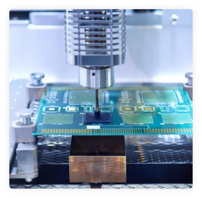
Manufacturing Excellence
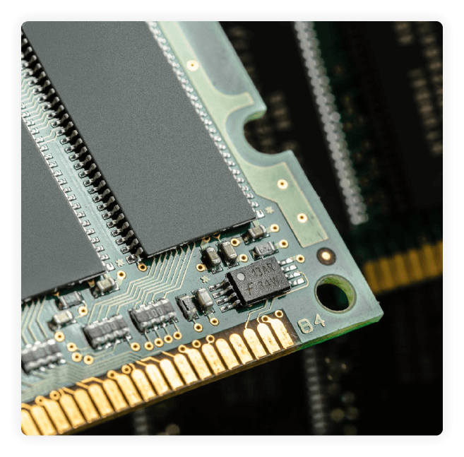
Custom High-Frequency PCB
Custom High-Frequency PCB
Manufacturing & RF Assembly Services
-
Thermal Stability
Optimized for extreme temperature fluctuating environments.
-
Precision Soldering
Professional SMT and Thru-Hole assembly for 01005+ components.
-
Advanced Testing
Comprehensive ICT, FCT, and 3D X-Ray Inspection protocols.
-
Global Compliance
Fully certified with UL, CE, FCC, and RoHS standards.