22
Dez.
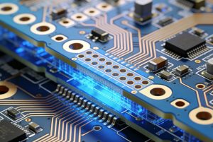
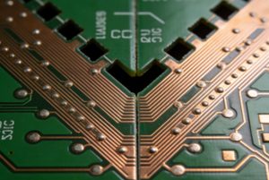
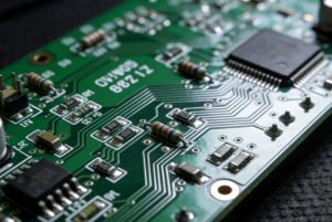
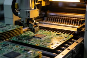
PCB Manufacturing vs PCB Assembly: What’s the Difference?
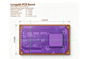
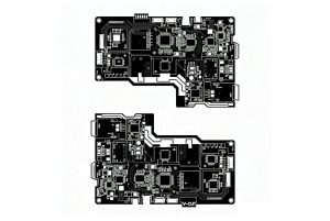
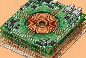
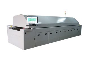
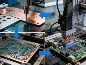
Lernen Sie die klaren Unterschiede zwischen der Leiterplattenherstellung und der Leiterplattenbestückung kennen. Bei der Herstellung wird die unbestückte Leiterplatte durch Ätzen und Schichten hergestellt, während sie bei der Bestückung (PCBA) mit...