Angebot einholen
UNSER BLOG
Konzentrieren Sie sich auf die neuesten Artikel, die Themen von den neuesten Technologien bis hin zu Best Practices und Branchennachrichten für PCB abdecken.
Apr. 02, 2026
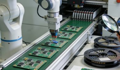
Selecting the right PCBA supplier is crucial for ensuring your electronics project meets quality, cost, and timeline goals. This article examines the factors that distinguish reliable suppliers, including technical expertise, quality systems, material selection, process control, and communication. With actionable how-to guidance and real-world considerations, engineers and project managers can make informed supplier decisions.
März 24, 2026
März 23, 2026
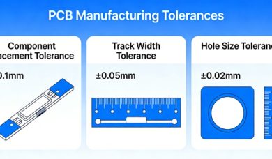
Lernen Sie wichtige Toleranzen bei der Leiterplattenherstellung kennen, die sich auf Ausbeute, Kosten und Zuverlässigkeit auswirken. Fachkundige Einblicke vom professionellen Hersteller TOPFAST. Unverzichtbarer Leitfaden für optimales Design und optimale Produktion.
26
Feb.
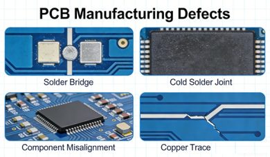
Dieser Artikel von TOPFAST beschreibt häufige Fehler bei der Leiterplattenherstellung, erläutert deren Ursachen und stellt wichtige Präventionsstrategien vor, um die Zuverlässigkeit und Ausbeute der Leiterplatten sicherzustellen.
22
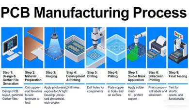
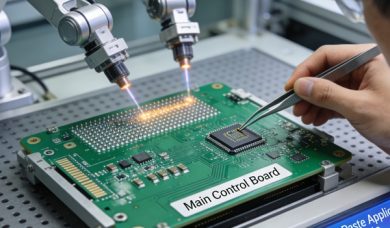
TOPFAST erläutert den gesamten Prozess der Leiterplattenherstellung. Er beginnt mit einer Designprüfung, gefolgt von Schritten wie Belichtung, Ätzen und Laminieren der Schichten. Der Prozess endet mit gründlichen elektrischen Tests und einer Endkontrolle, um Qualität und Zuverlässigkeit sicherzustellen.
18
Lesen Sie echte Bewertungen und Erfahrungsberichte zur Leiterplattenbestückung. Erfahren Sie, warum Ingenieure weltweit auf TOPFAST vertrauen, wenn es um zuverlässige, hochwertige PCBA-Dienstleistungen und erfolgreiche Projektpartnerschaften geht.
14
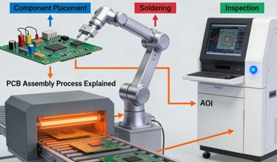
Reale Fallstudien zur Leiterplattenbestückung zeigen den Weg vom Prototyp bis zur Produktion. Entdecken Sie, wie TOPFAST zuverlässige PCBA-Lösungen für verschiedene Branchen liefert und dabei in jeder Phase Qualität und Effizienz gewährleistet.
10
Wir vergleichen TOPFAST mit JLCPCB, PCBWay und NextPCB im Bereich der Leiterplattenbestückung. Zu den wichtigsten Faktoren zählen Kosten, Vorlaufzeit, Qualität, Flexibilität und PCBA-Support, damit Sie den für Ihre Projektanforderungen am besten geeigneten Service auswählen können.
08
Diese FAQ des Leiterplattenherstellers TOPFAST behandelt wichtige Aspekte der Leiterplattenbestückung, darunter Kosten, Vorlaufzeiten, erforderliche Dateien, Testoptionen und schlüsselfertige Dienstleistungen sowohl für Prototypen als auch für die Produktion.
05
Erfahren Sie mehr über die wichtigsten Kriterien für die Auswahl eines Herstellers von Leiterplattenbaugruppen. Dieser Leitfaden behandelt wichtige Zertifizierungen, Kostenanalysen, die Bewertung von Vorlaufzeiten und einen schrittweisen Prozess zur Sicherstellung einer zuverlässigen Partnerschaft.
02
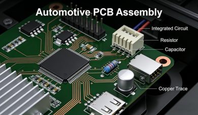
Die Montage von Leiterplatten für die Automobilindustrie erfordert die strikte Einhaltung der IATF 16949-Normen. Sie erfordert robuste Testmethoden und spezielle Best Practices, um höchste Zuverlässigkeit und Leistung in anspruchsvollen Fahrzeugumgebungen zu gewährleisten.
31
Jan.
Fordern Sie ein Angebot für Leiterplatten/PCBA an, indem Sie Ihre Gerber-, Stücklisten- und Bestückungsdateien einreichen. TOPFAST bietet Ihnen von Ingenieuren geprüfte Preise, klare Lieferzeiten und umfassende Fertigungsunterstützung für Ihr Projekt.
30
Die industrielle Leiterplattenbestückung erfordert strenge Standards hinsichtlich der Zuverlässigkeit. Dieser Überblick behandelt die wichtigsten Anforderungen, Fertigungsprozesse, strengen Prüfverfahren und bewährten Verfahren der Branche, um robuste und langlebige industrielle Leiterplattenbestückungen zu gewährleisten.
29
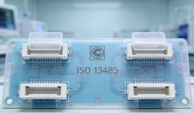
Die Montage medizinischer Leiterplatten erfordert die strikte Einhaltung von Normen wie ISO 13485. Dazu gehören strenge Prüfverfahren und spezielle bewährte Verfahren, um höchste Zuverlässigkeit und Sicherheit für kritische medizinische Geräte zu gewährleisten.
27
Load More
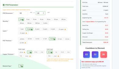
Schichten 1 Lagen 2 Lagen 4 Lagen 6 Lagen 8 Lagen 10 Lagen 12 Lagen 14 Lagen
Abmessungen (mm)
Menge 5 10 15 20 25 30 35 40 50 75 100 100+
Dicke 0,4 mm 0,6 mm 0,8 mm 1,0 mm 1,2 mm 1,6 mm 2,0 mm 2,4 mm
Menge
Anzahl der Einzelteile
SMT-Pads
Durchgangslöcher