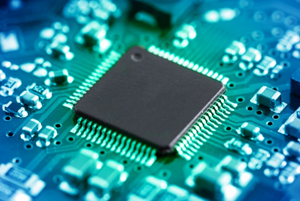
In the field of electronic engineering, PCB (Printed Circuit Board) as the core component of electronic equipment, its design quality is directly related to the performance, reliability and productivity of the equipment. During the design process, engineers often encounter a variety of challenges, which, if not handled properly, will have a negative impact on the entire system. The following is an in-depth analysis of common problems in PCB design, and provide targeted solutions to help designers avoid potential risks and improve design quality.
Table of Contents
1.Component layout is not reasonable
Problems
Component layout if too dense, will increase the probability of interference between signals, while impeding the distribution of heat, resulting in high local temperatures; while the layout is too dispersed, will result in an increase in the length of the wiring, not only a waste of space on the board, but also the possible introduction of additional signal delay and noise. In addition, the unreasonable layout will also make the subsequent wiring work difficult to meet the design requirements.
The Solution
Functional Modular Layout: Layout is partitioned according to the functional modules of the circuits, and high-frequency circuits are strictly separated from low-frequency circuits. For example, in the PCB design of wireless communication equipment, RF modules and baseband processing modules are arranged in different areas of the board to reduce the interference of high-frequency signals to low-frequency signals.
Optimize the heat dissipation layout: Keep the heat-generating components at an appropriate distance from the sensitive devices to avoid performance degradation of the heat-sensitive components due to high temperature. At the same time, reserve sufficient heat dissipation space for the heat-generating components, and can adopt auxiliary heat dissipation measures such as heat dissipation holes and heat sinks.
Priority layout of key devices: In the layout, the priority to determine the location of key devices (such as CPU, memory chips, etc.), the layout of these devices directly affects the signal integrity and system performance. Take the computer motherboard design as an example, the location of the CPU determines the direction of high-speed signal wiring such as memory, graphics card, etc. Reasonable layout of the CPU can effectively reduce signal delay and interference. Determine the location of key devices, and then gradually arrange the peripheral components to ensure that the overall layout is compact and reasonable.
2.Signal Integrity Problems
Problem Performance
Signal reflection, crosstalk or delay phenomena can occur during signal transmission due to impedance mismatch, too long of alignment, too many over-holes and other factors, resulting in signal distortion, which in turn triggers communication errors.
These problems are especially prominent in high-speed digital circuits, which may cause data transmission errors, system crash and other serious consequences.
The Solution
Differential pair design: For high-speed signal lines (e.g. USB, HDMI, etc.), a differential pair design is used. Differential signals are transmitted through two signal lines with opposite polarity, which has strong anti-interference ability, can effectively suppress common mode noise, and improve the accuracy and stability of signal transmission.
Control alignment impedance matching: Ensure that the characteristic impedance of the alignment matches the impedance of the signal source and load to avoid signal reflection. In the design process, the impedance can be controlled by adjusting the alignment width, dielectric thickness and other parameters. At the same time, try to avoid right-angle alignment, because right-angle alignment will change the characteristic impedance of the alignment, resulting in signal reflection and radiation.
Optimize the reference layer design: Adding termination resistors or using a ground plane as a reference layer can effectively absorb reflected signals and reduce signal noise. The ground plane not only provides a good return path for the signal, but also serves as a shield against interference.
3.Signal cascade design is not reasonable
Problem Performance
Improperly designed signal stacking can lead to increased signal crosstalk and degradation of signal transmission quality. Especially in multi-layer PCB design, unreasonable stacking order may cause high-speed signals to be interfered with, affecting the overall performance of the system.
For example, if the high-speed signal layer is adjacent to the power supply layer, it is easy to introduce power supply noise to interfere with signal transmission.
Solution
Follow the principle of layer-stacking design: Plan the layer-stacking structure according to the signal type and frequency, generally place the high-speed signal layer in the middle layer, and isolate it through the ground plane or power plane. For example, in an 8-layer board design, layers 2 and 7 can be set as ground planes, while layers 3 and 6 are used for high-speed signal transmission to effectively reduce signal crosstalk.
Control of dielectric thickness and dielectric constant: Reasonable selection of the dielectric thickness and dielectric constant of the circuit board substrate to optimize the characteristic impedance of signal transmission and transmission delay. For high-speed signals, low dielectric constant boards can be used to reduce signal loss.
4.Hole design is not standardized
Problems
Unreasonable size, excessive number or improper layout of vias will increase the loss and reflection of signal transmission and affect signal integrity. For example, the mismatch between the aperture of the vias and the size of the pads may lead to poor soldering; a large number of vias concentrated in the high-speed signal path will introduce additional parasitic capacitance and inductance.
The Solution
Optimize via parameters: Select the appropriate via aperture, pad size and drilling depth according to the signal frequency and current. For high-frequency signals, minimize the size of the vias and use blind or buried hole designs to reduce signal loss.
Reasonable planning of over-hole layout: avoid dense distribution of over-holes on the high-speed signal path, and decentralize the location of over-holes to reduce the impact on signal transmission. At the same time, make sure the connection between the over-hole and the signal line is smooth and avoid right-angle connection.
5.Insufficient power integrity
Problems
Excessive power supply noise, voltage dips and other problems can seriously affect the stability of the system. Power supply noise may interfere with the normal operation of sensitive circuits, resulting in signal distortion; while voltage drops may prevent the chip from working properly, resulting in crashes, reboots and other phenomena.
Solution
Multilayer board design: A multilayer board design is used, specializing in power and ground planes. The multilayer board can provide a large plane area for the power supply and ground, lowering the impedance of the power supply and ground and reducing power supply noise. At the same time, the capacitance formed between the power supply and ground plane can also play a role in filtering, further improving the stability of the power supply.
Reasonable placement of decoupling capacitors: decoupling capacitors are placed near the power inlet and chip, decoupling capacitors can quickly respond to the transient current demand of the chip and suppress power supply noise. Generally speaking, for different frequency noise, need to choose different capacitance decoupling capacitors for filtering.
Optimize the power path: Use wide traces or copper to lower the impedance of the power path and reduce the voltage drop. Wide alignment and copper paving can provide greater current carrying capacity and ensure that the power supply can stably supply power to each component.
6.Electromagnetic compatibility (EMC) problems
Problem performance
Circuit board radiation exceeds the standard will produce interference with the surrounding electronic equipment, and poor interference immunity is easy to make the circuit board by the external electromagnetic interference, resulting in system performance degradation or even can not work properly.
Solution
Signal isolation layout: keep sensitive signals away from clock lines and power lines, because clock lines and power lines are the main source of electromagnetic interference. Through a reasonable layout, reduce the coupling between sensitive signals and interference sources to reduce the impact of electromagnetic interference.
Shielding treatment: Shield the high-frequency circuits. Metal shielding cover or shielding mesh can be used to close the high-frequency circuits to prevent the leakage of electromagnetic radiation, and at the same time, it can also resist the external electromagnetic interference.
Ensure the integrity of the ground plane: Ensure the integrity of the ground plane to avoid splitting resulting in a broken return path.
A complete ground plane can provide a good return path for the signal and reduce electromagnetic radiation. In the design process, try to avoid splitting the ground plane under important signals.
7.High-speed interface compatibility issues
Problem Performance
With the widespread use of high-speed interfaces (such as PCIe, Thunderbolt, etc.), interface compatibility issues are becoming more and more prominent. Failure of interface design to comply with specifications may lead to problems such as unrecognizable equipment, reduced or unstable data transfer rates, etc.
Solution
Strictly follow the interface standards: When designing high-speed interface circuits, thoroughly study and strictly follow the relevant standards to ensure that the electrical characteristics of the interface, signal timing, etc. meet the requirements. For example, when designing PCIe interfaces, it is necessary to design them in strict accordance with the signal topology and impedance matching requirements stipulated in the PCIe protocol.
Signal integrity verification: Use simulation tools to analyze the integrity of high-speed interface signals, simulate signal transmission under different working conditions, and discover and solve potential problems in advance. At the same time, in the actual test phase, the use of professional test equipment to comprehensively test the interface performance to ensure interface compatibility and stability.

8.Defective heat dissipation design
Problem Performance
Excessive local temperature will accelerate the aging of the device, reduce the life of the device, and may even lead to device failure, affecting the reliability of the entire system.
Solution
Add heat dissipation holes: Add heat dissipation holes under the heat generating components, the heat dissipation holes can quickly conduct the heat to the other side of the board, increase the heat dissipation area and improve the efficiency of heat dissipation.
Auxiliary heat dissipation measures: According to the actual demand, use heat sinks or fans to assist in heat dissipation. Heat sinks can increase the heat dissipation area and accelerate the heat dissipation; fans can take away the heat from the circuit board by forced convection.
Thermal simulation analysis: In the design stage, through the simulation software to analyze the thermal distribution in advance, to understand the temperature of the circuit board in different working conditions, so as to optimize the heat dissipation design, to ensure that the temperature of the circuit board within a reasonable range.
9.Production manufacturability issues
Problems
If the design does not meet the PCB manufacturer’s process requirements, it will lead to various problems during the production process, such as poor soldering, short circuits, etc., which will increase the production cost and prolong the production cycle.
The Solution
Follow the design rules: Before designing, fully understand the design rules provided by PCB manufacturers (e.g., minimum line width, aperture diameter, etc.), and design in strict accordance with the rules to ensure the manufacturability of the design.
Optimize pad design: Avoid too small a pad spacing to prevent bridging when soldering. Reasonable design of the shape, size and spacing of the pads can improve soldering quality and reduce the rate of soldering defects.
Add process auxiliary elements: Add process edges and positioning holes to facilitate assembly, process edges can provide convenience for PCB processing, testing and assembly, and positioning holes are used to ensure the positional accuracy of the PCB in the process of processing and assembly.
10.Test and debugging difficulties
Problem Performance
Lack of test points will make troubleshooting difficult, engineers are difficult to accurately determine the location of the fault, increasing debugging time and cost.
Solution
Reserve test points: Reserve test points on key signal lines, which should be easy for probes to contact and have good electrical performance. Through the test points, engineers can easily measure the signal voltage, waveform and other parameters, and quickly locate the fault.
Use of standard interfaces: Use standard interfaces (such as JTAG) for program debugging. Standard interfaces are universal and standardized, and can be easily connected to debugging equipment to improve debugging efficiency.
Consider the test space: Consider the probe contact space in the design phase to ensure that the test equipment can smoothly contact the test point, to avoid not being able to test due to lack of space.
Summary
PCB design is a comprehensive and highly systematic project that requires comprehensive consideration of various factors such as electrical performance, mechanical structure and production process. By identifying and solving common problems in advance, it is possible to significantly reduce the number of design iterations and improve product reliability and stability.
In the design process, it is recommended that designers make full use of EDA tools for simulation and analysis, to identify potential problems in advance and optimize the design scheme. At the same time, and PCB manufacturers to maintain close communication, timely understanding of the production process requirements, to ensure that the design can be successfully realized. Only in this way can we design high-quality PCBs to meet the increasingly complex functional requirements of modern electronic devices.