24
Oct
What is an aluminum-based PCB?
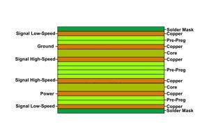
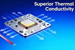
Aluminum-based PCBs (aluminum printed circuit boards) are specialized printed circuit boards utilizing aluminum alloy as the substrate material. Their three-layer structural design delivers exceptional thermal...