6
Apr
Turnkey PCBA Supplier: How to Source Complete Assembly Services
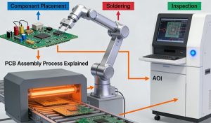
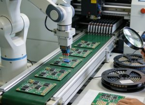
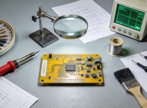
Turnkey PCBA services simplify electronics manufacturing by combining PCB fabrication, component sourcing, assembly, and testing into a single workflow. This article explains how turnkey suppliers...