Get a Quote
OUR BLOG
Focus on the latest articles that cover topics ranging from the latest technologies to best practices and industry news for PCB.
Mar 18, 2026
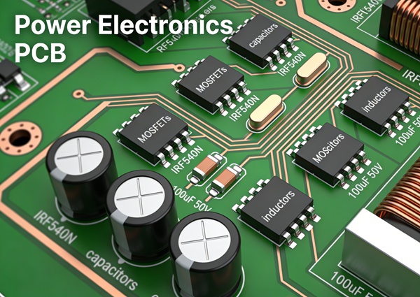
This article explores key design strategies for EV power electronics PCBs, including copper thickness selection, thermal management techniques, high-voltage spacing considerations, and stack-up optimization. It also discusses how PCB structure influences assembly reliability, particularly in high-power components and multilayer boards.
Mar 14, 2026
Mar 12, 2026
This document outlines the fundamental concepts and classification system of electronic components, provides a detailed analysis of the functional characteristics and distinctions between passive and active components, introduces quality grading standards and key selection criteria for components, and addresses common application issues.
11
Oct
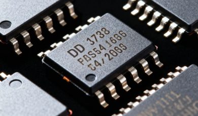
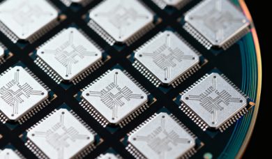
Integrated circuits (ICs) are miniature electronic devices that integrate components such as transistors, resistors, and capacitors onto a single chip through semiconductor processes. This comprehensive analysis explores the working principles of integrated circuits, from the operational mechanisms of their core building blocks—transistors—to complex hierarchical structural designs. It provides detailed explanations of various classification methods, including categorization by function, integration level, and application domain.
09
Fundamental circuit concepts, including the nature of electricity, the relationship between voltage and current, and the distinction between AC and DC power. Emphasis is placed on constructing simple LED circuits, with detailed analysis of techniques for identifying and resolving two common faults: short circuits and open circuits.
29
Sep
A comprehensive PCBA production quality control system encompasses critical aspects such as raw material management, production process control, advanced inspection technology application, and employee training. By implementing thorough quality control measures, electronics manufacturing enterprises can significantly enhance product yield rates and market competitiveness.
27
Beyond a mere technology showcase, Iran Elecomp 2025 reveals critical shifts in the Middle Eastern electronics landscape. Our analysis identifies three core trends: the market's maturation towards demanding integrated solutions, the strategic push for technological sovereignty and localized partnerships, and the convergence of performance and sustainability.
25
This comprehensive analysis examines the technical characteristics and application scenarios of flexible PCB materials, focusing on the performance differences and selection strategies for four major flexible substrates: polyimide (PI), polyester (PET), polyethylene naphthalate (PEN), and liquid crystal polymer (LCP).
24
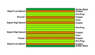
PCB power planes are a core component of modern electronic devices, directly impacting system performance, stability, and reliability. This encompasses all aspects from fundamental concepts to advanced techniques, including critical elements such as layering strategies, power partitioning, via design, mixed-signal processing, and thermal management.
19
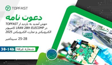
The 2025 Iran Electronics Exhibition will be held in Tehran this September, showcasing electronic components, PCBs, semiconductor packaging, and smart manufacturing equipment. The event features professional forums and business matching platforms to help companies expand into the Middle East market. Key exhibitor Topfast will present its innovative PCB solutions and specialized technical services.
17
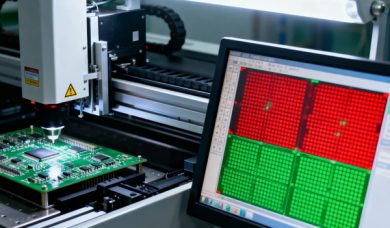
PCB defect detection is a critical process in electronics manufacturing. This paper systematically investigates the principles and characteristics of optical, electrical, thermal imaging, X-ray, and acoustic detection technologies. Through comparative analysis, it proposes recommendations for technology selection and explores future trends in artificial intelligence and multimodal fusion.
15
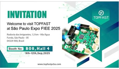
The 2025 FIEE Brazil Exhibition is currently underway at the São Paulo Exhibition and Convention Center. This year's event features dedicated zones for hot topics like photovoltaic energy storage and automation robotics, showcasing products and technologies across the entire industry chain and attracting participation from global industry leaders. Topfast is also exhibiting at the show, offering high-end PCB manufacturing and electronic solutions.
Selecting the number of PCB layers is a critical decision in electronic design, directly impacting product performance and cost. This paper systematically analyzes the theoretical limits and practical manufacturing constraints of PCB layer counts, providing a detailed comparison of the advantages, disadvantages, cost structures, and application scenarios for different layer counts (4 to 32 layers).
Incoming material inspection for printed circuit boards is a critical step in ensuring electronic product quality. This guide covers the conditions, items, methods, and tools for PCB inspection, encompassing the entire process from visual and dimensional checks to electrical and reliability testing. It includes solutions to common issues and references to industry standards, providing practical guidance for companies to establish an efficient incoming material inspection system.
04
Load More
Layers 1 Layers 2 Layers 4 Layers 6 Layers 8 Layers 10 Layers 12 Layers 14 Layers
Dimensions (mm)
Quantity 5 10 15 20 25 30 35 40 50 75 100 100+
Thickness 0.4mm 0.6mm 0.8mm 1.0mm 1.2mm 1.6mm 2.0mm 2.4mm
Quantity
Number of Unique Parts
SMT Pads
Thru-Holes