Expert Service
Advanced PCB Reverse Engineering Solutions
From physical board analysis to complete schematic recreation and PCB redesign
99.9%
Accuracy Rate
5-10 Days
Fast Turnaround
1000+
Projects Completed
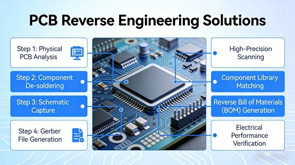
Our Reverse Engineering Process
Step-by-step approach to ensure accurate and reliable PCB cloning
01
Board Analysis & Documentation
Physical inspection, high-resolution imaging, and comprehensive documentation of original PCB
- High-resolution photography
- Component identification
- Layer stack-up analysis
02
Schematic Recreation
Complete circuit schematic recreation with netlist verification and component connectivity mapping
- Circuit analysis
- Netlist extraction
- Schematic verification
03
PCB Layout Design
Professional PCB layout design with signal integrity optimization and manufacturability considerations
- Layout recreation
- Signal integrity check
- DFM optimization
04
Verification & Testing
Comprehensive testing and verification to ensure cloned PCB matches original functionality
- Functional testing
- Performance comparison
- Quality validation
Our Technical Capabilities
Advanced equipment and expertise for complex PCB reverse engineering
Multi-layer PCB Analysis
Expert analysis of complex multi-layer PCBs up to 32 layers with blind/buried vias
Up to 32 layers
HDI boards
Flexible PCBs
Component Identification
Advanced component identification including BGA, QFN, and miniaturized SMD components
BGA/QFN
Micro BGA
0201/01005
Signal Integrity Analysis
Comprehensive signal integrity analysis for high-speed and RF circuit designs
High-speed
RF circuits
Impedance control
Design Optimization
Professional design optimization for manufacturability and performance enhancement
DFM optimization
Cost reduction
Performance boost
Application Scenarios
Where PCB reverse engineering adds value to your business
Legacy Product Support
Revive discontinued products by recreating schematics and PCBs when original documentation is lost or manufacturers no longer exist.
- No original documentation needed
- Component sourcing assistance
- Design documentation recreation
Competitive Analysis
Analyze competitor products to understand their design approach, component selection, and manufacturing techniques.
- Design methodology analysis
- Cost structure evaluation
- Performance benchmarking
Product Improvement
Enhance existing designs by analyzing current PCBs and implementing improvements in performance, cost, or reliability.
- Performance optimization
- Cost reduction analysis
- Reliability enhancement
Failure Analysis
Identify design flaws and manufacturing defects through detailed analysis of failed PCBs to prevent future issues.
- Root cause identification
- Design flaw detection
- Manufacturing defect analysis
Ready to Start Your PCB Reverse Engineering Project?
Send us your PCB sample for a free feasibility analysis and detailed quote
Free Feasibility Analysis
Get a free assessment of your PCB cloning project complexity and requirements
Detailed Project Quote
Receive a comprehensive quote with timeline, cost breakdown, and deliverables
NDA Protection
Your design and intellectual property are protected with signed NDA agreements
Response within 4 hours | Free project assessment | Confidentiality guaranteed