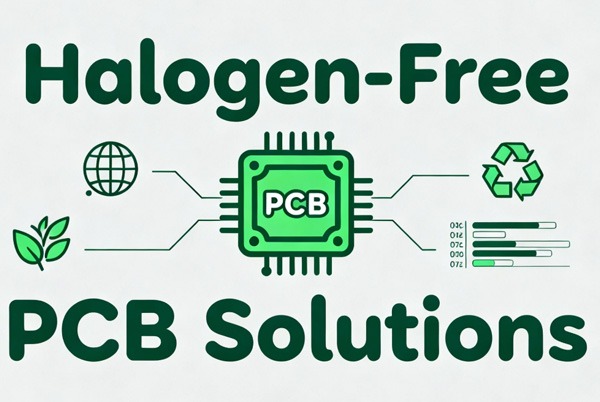
In today’s pursuit of high performance and miniaturization, electronic engineers face a new core challenge: how to make designs more environmentally friendly and safer? Halogen-free PCBs are the key solution to this challenge. They have evolved from an optional specification into an essential requirement for accessing global markets and earning consumer trust.
Table of Contents
What is a Halogen-Free PCB?
Simply put, a Halogen-Free PCB is a printed circuit board that strictly limits the content of halogens (specifically bromine and chlorine) in its substrate, flame retardants, and other parts.
According to the authoritative definition by the International Electrotechnical Commission (IEC) standard IEC 61249-2-21, a PCB must meet all the following conditions to be called “halogen-free”:
- Bromine (Br) content ≤ 900 ppm
- Chlorine (Cl) content ≤ 900 ppm
- Total Halogen content ≤ 1500 ppm
This standard aligns with the halogen limit requirements in the EU’s Restriction of Hazardous Substances (RoHS) Directive. This means that adopting halogen-free PCBs is not just an environmental choice but a smart move to ensure product compliance with major global market regulations.
Why Choose Halogen-Free PCBs?
Switching to halogen-free PCBs isn’t just for a “green” label; it offers tangible performance and reliability improvements for your products.
- Environmental Safety and Sustainability
Traditional halogenated flame retardants release potent carcinogens like dioxins and furans when burned or improperly disposed of. Halogen-free materials eliminate this risk at the source, significantly reducing the negative environmental impact of electronics throughout their lifecycle. - Superior Performance
- Higher Thermal Stability: Halogen-free laminates typically have a higher Glass Transition Temperature (Tg), often above 150°C, which enables them to better withstand the high temperatures of lead-free soldering processes and high-temperature operating environments, thereby reducing delamination risks.
- Better Electrical Properties: Many halogen-free materials possess a lower Dielectric Constant (Dk) and Dissipation Factor (Df). This is crucial for signal integrity in high-frequency, high-speed circuits (e.g., 5G, RF applications), effectively reducing signal attenuation.
- Strong Regulatory and Market Access
Meeting standards like IEC and RoHS is a ticket to enter markets like the EU. Furthermore, products with a “halogen-free” identifier are more competitive in automotive, telecommunications, and high-end consumer electronics, serving as powerful proof of a brand’s environmental commitment. - Enhanced Long-Term Reliability
Halogen-free PCBs often exhibit lower moisture absorption (can be below 0.1%), enhancing their reliability in humid environments and reducing failure risks like open or short circuits caused by moisture uptake, thereby extending product lifespan.
Environmental Impact of Halogenated PCBs
Halogens, especially brominated flame retardants, were widely used for their effective flame resistance, but at a great cost:
- Toxic Emissions: During fires or recycling incineration, they release large amounts of corrosive and toxic gases, polluting the air and soil.
- Recycling Difficulties: Processing halogenated waste is complex and costly, easily leading to improper disposal and worsening environmental burdens.
How to Choose Halogen-Free Laminates?
With various halogen-free materials available, how do you make the right choice? Focus on these key factors:
- Material System: Mainstream halogen-free materials use Phosphorus (P), Nitrogen (N), or P-N synergistic systems as flame retardants.
- Key Parameters:
- Thermal Performance: Focus on Tg (>150°C is better) and Decomposition Temperature (Td).
- Electrical Performance: For high-frequency applications, choose materials with low Dk (e.g., <3.5) and low Df (e.g., <0.005).
- Mechanical Properties: Ensure peel strength and toughness meet assembly and usage requirements.
- Cost and Supply Chain: Halogen-free materials may cost 10%-20% more. Balance the budget with performance needs and choose reliable suppliers with stable stock.
Design Transition Challenges and Smooth Transition Solutions
Acknowledging challenges is the first step to a successful transition. Halogen-free PCB design may face:
- Increased Costs: Material and potential process adjustments increase costs.
- Process Adjustments:
- Drilling: Materials are harder, potentially requiring adjusted drilling parameters.
- Etching: Slightly lower alkali resistance requires controlled immersion time in alkaline solutions to prevent substrate whitening.
- Assembly: Halogen-free PCBs often use lead-free processes, requiring higher reflow soldering peak temperatures (around 260°C).
Five-Step Smooth Transition Process:
- Needs Assessment: Define regulatory and client requirements for the target market.
- Material Research: Work closely with suppliers to screen laminates meeting specifications.
- Prototype Testing: Build and thoroughly test prototypes to verify manufacturability (DFM) and reliability.
- Process Update: Communicate with manufacturers to optimize parameters for drilling, soldering, etc.
- Team Enablement: Ensure design and production teams understand new material properties and handling requirements.
Frequently Asked Questions (FAQ)
- Q: Are Halogen-Free and RoHS the same thing?
- A: No. RoHS primarily restricts Lead, Mercury, Cadmium, Hexavalent Chromium, PBB, and PBDE. Halogen-Free specifically restricts Chlorine and Bromine content. They are independent but complementary concepts often required simultaneously.
- Q: Is Halogen-Free mandatory?
- A: There is currently no unified global law mandating it, but it has become a de facto standard in many industries (especially automotive and consumer electronics), driven by strong market demand.
- Q: Why do standards only restrict Chlorine and Bromine?
- A: Because among halogens, Chlorine and Bromine (especially Bromine) are the most commonly used in flame retardants for electronics; Fluorine, Iodine, etc., are rarely used.
Conclusion
Halogen-free PCBs are no longer a future concept but a present-day design necessity. They represent the perfect balance that the electronics industry has achieved between performance, safety, and sustainability. For forward-thinking engineers, proactively understanding and applying halogen-free PCB technology is not just about mitigating regulatory risks but also about shaping more competitive and responsible products.