Table of Contents
PCB Schematic File Types
1. Schematic Design Files
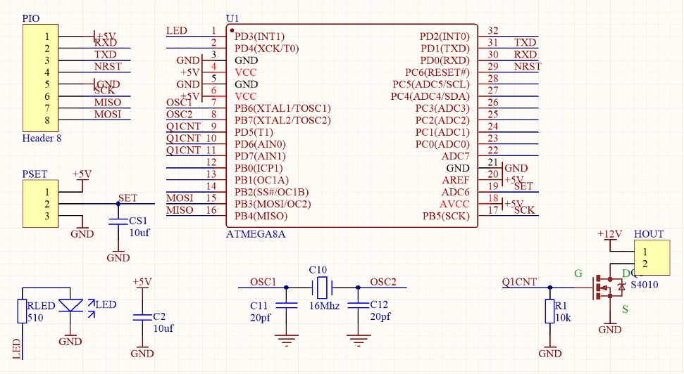
- .SCH Files: Standard schematic files defining component connections (used in Protel, Altium Designer, KiCad).
- .SchDoc Files (Altium Designer): Modern schematic source files supporting hierarchical design.
- .DSN Files (Cadence OrCAD): Contain schematic designs and project management data.
2. PCB Layout Files
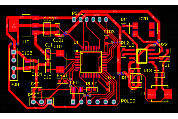
- .PCB/.PCBDoc Files (Altium Designer): Store physical design data (component placement, routing, stack-up).
- .BRD Files (Cadence Allegro, Eagle): Industry-standard format for high-density PCB designs.
- .PADS Files (Mentor Xpedition/PADS): Used for professional PCB layout and manufacturing output.
3. Key Manufacturing Files
- Gerber Files (.gbr/.ger):
- RS-274X format (e.g., TopLayer.gbr, SilkScreen.gbr) defines copper, solder mask, and silkscreen layers.
- Must include all critical layers for fabrication.
- Drill Files (.drl/.txt):
- Excellon format specifies hole locations and sizes (must match Gerber files).
- IPC-356 Netlist: Ensures electrical consistency between schematics and PCB layout.
- BOM (.csv/.xlsx): Include reference designators, part numbers, quantities, and supplier details.
PCB Manufacturing File Checklist
- Design Verification:
- Run DRC (Design Rule Check) and ERC (Electrical Rule Check).
- Confirm layer stack-up and impedance requirements.
- File Compatibility:
- Export Gerber in RS-274X (avoid outdated RS-274D).
- Provide ODB++ (.tgz) or IPC-2581 for better data exchange.
- Manufacturing Requirements:
- Specify board thickness, surface finish (ENIG, HASL), and solder mask color.
- Include assembly drawings (.PDF) and 3D models (.STEP) for better collaboration.
Frequently Asked Questions (FAQs)
❓ “How much does PCB manufacturing cost?”
Cost depends on board size, layers, material, and finish. Example:
- 2-layer FR4 (10×10cm): ~$5 for 10pcs (standard specs).
- HDI (blind/buried vias): Higher cost—request a detailed quote.
❓ “What’s the difference between Gerber and ODB++ files?”
- Gerber: Standard 2D image files for each PCB layer.
- ODB++: A structured database format containing all PCB data (better for complex designs).
❓ “How do I ensure my PCB design is manufacturable?”
- Follow DFM (Design for Manufacturing) guidelines.
- Verify minimum trace width, hole size, and clearance with your PCB fab.
❓ “Can I use KiCad files for professional manufacturing?”
- Yes! Most manufacturers accept export Gerber, drill files, and BOM.
- Avoid sending native
.kicad_pcbfiles; standardized formats are preferred.