Miniaturization in PCB manufacturing process refers to the ongoing trend of designing and producing smaller and more compact printed circuit board for various electronic devices. This phenomenon has been driven by the ever-increasing demand for smaller and more portable electronic products across industries such as consumer electronics, healthcare, automotive, and aerospace.
Table of Contents
The Drive for Miniaturization
Consumer Electronics: The demand for smaller and lighter consumer devices, such as smartphones, tablets, and wearables, has been a primary driver of miniaturization in PCBs. Consumers seek sleek, portable gadgets with powerful features.
Medical Devices: Miniaturization plays a crucial role in the development of medical devices like pacemakers, implantable sensors, and diagnostic equipment, allowing for minimally invasive procedures and enhanced patient comfort.
Automotive Industry: Automotive manufacturers are incorporating smaller PCBs into vehicles to reduce weight, improve fuel efficiency, and enable advanced driver assistance systems (ADAS) and autonomous driving technologies.
Aerospace and Defense: Space-constrained environments in aerospace applications necessitate miniaturized PCBs to reduce weight and maximize functionality, ensuring reliable performance in extreme conditions.
Miniaturization Solutions
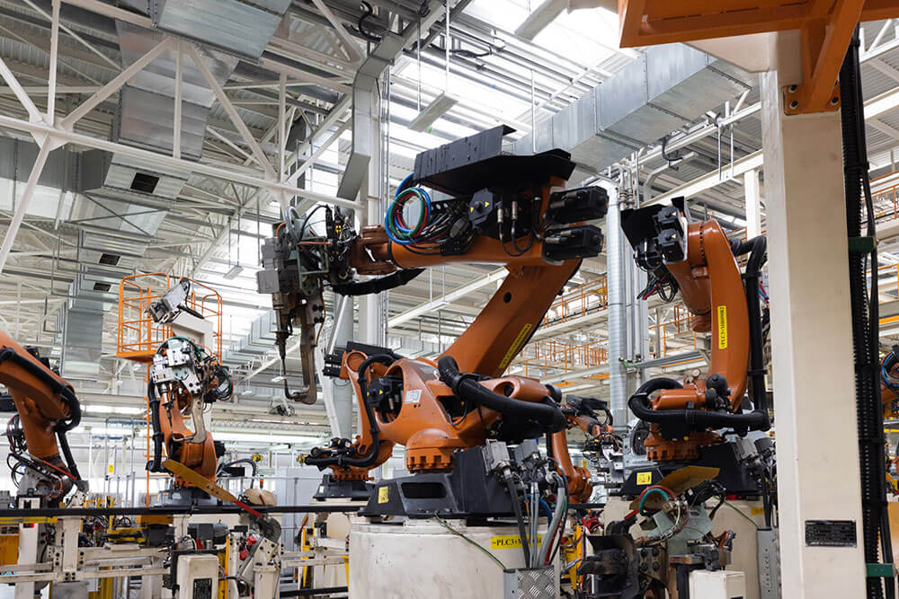
Surface Mount Technology (SMT): Surface Mount Technology (SMT) has revolutionized PCB fabrication by reducing PCB board size while enhancing performance. This method eliminates the need for through-hole components, allowing for smaller and more compact PCBs. SMT achieves this through higher component density, the use of smaller components, shorter trace lengths, and precise component placement. This technology finds wide-ranging applications in consumer electronics, medical devices, automotive systems, and aerospace, enabling the creation of sleeker and more efficient electronic devices. However, it also presents challenges in terms of design complexity and the need for specialized equipment, which must be carefully managed to fully exploit the benefits of miniaturization through SMT.
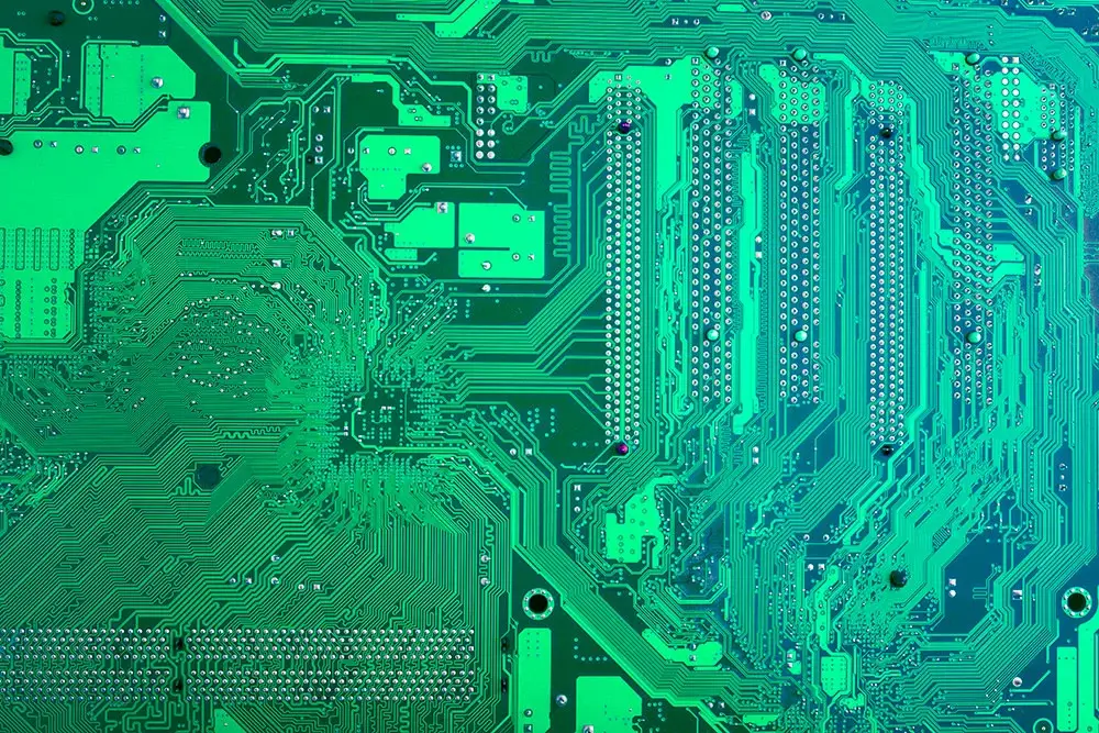
High-Density Interconnects (HDI): HDI Pcb (HDI) technology is a pivotal advancement in PCB manufacturing, enabling the creation of smaller and more efficient PCBs. HDI achieves this by allowing components to be placed closer together, reducing the board’s physical size while enhancing signal integrity and thermal management. This technology finds applications in various industries, including consumer electronics, medical devices, and automotive, where miniaturization is crucial for sleeker, high-performance devices. Despite its advantages, HDI PCB design complexity, manufacturing expertise, and potential cost increases are factors that must be carefully considered when implementing this technology for miniaturization.
Flexible PCB: Flexible PCBs, or flex printed circuit board, are a transformative technology revolutionizing circuit board design by dramatically reducing size while introducing unparalleled adaptability. Constructed from flexible materials like polyimide or polyester, they enable compact, three-dimensional designs and maximize component density, making them ideal for applications with space constraints. These lightweight and versatile PCBs find crucial roles in various industries, from wearables and medical devices to automotive systems and aerospace technology, where size reduction is essential. However, their design complexity and considerations related to durability and cost must be managed to fully capitalize on the benefits of miniaturization through flexible PCBs, which continue to reshape electronics and product innovation.
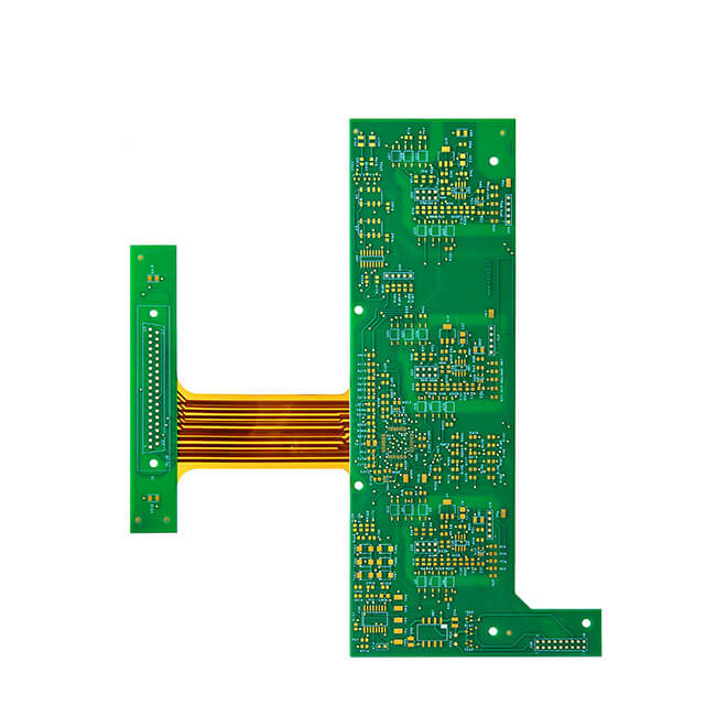
Rigid Flex PCB: Flex-rigid printed circuit board are a transformative technology in circuit board design, expertly balancing the need for miniaturization with structural integrity and reliability. Combining flexible layers with rigid sections, they enable three-dimensional layouts, optimizing every inch of available space, and accommodating high component density. This unique design results in smaller, compact boards ideal for industries such as consumer electronics, medical devices, automotive systems, and aerospace technology. Notably, they offer enhanced reliability by reducing potential points of failure, a key consideration in mission-critical applications. While design expertise and manufacturing costs remain considerations, the advantages of miniaturization through rigid flex PCB continue to drive their adoption, ushering in new possibilities in electronics and product innovation.
Benefits of Minimizing PCB
Enhanced Performance: Miniaturization allows for shorter signal paths, reducing signal degradation and enhancing the overall performance and speed of electronic devices.
Reduced Power Consumption: Smaller PCBs often require less power, which is essential for battery-powered devices like smartphones and IoT sensors.
Challenges in Manufacturing: While miniaturization offers numerous benefits, it also presents challenges in terms of component placement accuracy, thermal management, and the need for specialized pcb manufacturing equipment.
Increased Design Complexity: Miniaturization necessitates intricate PCB design, demanding sophisticated design software and thorough testing to ensure reliability.
Future Trends
5G Integration: The rollout of 5G networks will drive demand for miniaturized PCBs to support high-frequency, high-data-rate applications.

IoT Devices: As the Internet of Things (IoT) continues to expand, smaller PCBs will be crucial for embedding connectivity into everyday objects.
Nanotechnology: Advancements in nanotechnology may lead to even smaller electronic components and further miniaturization possibilities.
Miniaturization in PCB manufacturing is a transformative trend with far-reaching implications for the electronics industry. It enables the creation of smaller, more powerful, and energy-efficient electronic devices across a range of applications. However, it also presents challenges that engineers and manufacturers must address to ensure the reliability and functionality of miniaturized PCBs in an increasingly interconnected world.
Miniaturization with Topfast PCB
Topfast is your trusted PCB manufacturer when it comes to PCB assembly projects. With a team of highly skilled engineers and experts, Topfast not only excels in the manufacturing of PCB assemby but also specializes in finding innovative solutions for minimizing your PCB designs. Their engineers possess extensive knowledge and experience in optimizing circuit board layouts and component placements to achieve the most compact and efficient designs possible. Whether you’re working on consumer electronics, medical devices, automotive systems, or any other industry, Topfast’s commitment to excellence and their ability to provide tailored solutions can help you streamline your PCB assembly projects while ensuring top-notch quality and reliability.