Table of Contents
The Odyssey from Concept to Flex Circuit Board
Greetings, tech enthusiasts and innovators! Ever wondered about the incredible journey that transforms an idea into a flexible circuit board? Today, I’m thrilled to take you on an exhilarating voyage through the mesmerizing world of flex circuit board manufacturing. Brace yourself for a whirlwind tour from the inception of the design concept to the creation of a flexible circuit board ready for action.
Crafting in the Digital Realm
Our adventure begins with a voyage into the digital realm. Imagine skilled designers meticulously crafting layouts using advanced computer-aided design (CAD) systems. These CAD systems are powerful, but here’s the twist – each one has its unique internal data format. Enter the Gerber file, the standard output format that acts as the guiding star for transferring the layout data from the designer to the manufacturer. Consider it the blueprint that charts our course through this manufacturing odyssey.
Ensuring Feasibility with DFM
Before we embark on the manufacturing journey, there’s a critical checkpoint – the Design for Manufacturability (DFM) review. A CAD engineer painstakingly inspects trace widths, trace spacing, hole sizes, and more to ensure that the design aligns seamlessly with the manufacturing capabilities. Once the data passes the rigorous scrutiny, it’s time to set sail.
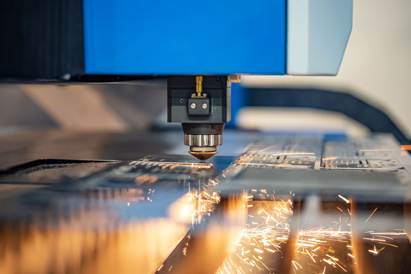
Illuminating the Darkroom
Now, let’s venture into the intriguing world of film creation for flex circuit boards. Picture a controlled environment where temperature and humidity reign supreme. Here, laser photo plotters convert the board data into pixel images and employ lasers to etch them onto films. But why this meticulous process? These films are the secret sauce that brings the flexible circuit board to life.
Inner Layers: Forging the Core
Multi-layer flex circuit boards are a marvel of engineering, and their creation begins with the preparation of a laminate panel. The process involves precise copper cleaning, the application of photosensitive film (photoresist), and the delicate alignment of films. UV lamps harden the photoresist, revealing the copper pattern we desire. However, before we move ahead, an operator meticulously checks that everything is pristine, ensuring a flawless foundation for what’s to come.
The Art of Etching
To unveil the copper pattern on inner layers, we undertake a meticulous etching process. Unwanted copper dissolves away through the power of a potent alkaline solution. It’s a precision task, and the operator ensures that every vestige of unwanted copper is meticulously removed. What remains is the exact pattern needed for your flex circuit board.
Precision Drilling and Plating – The Flex Circuit Transformation
Now, we’re diving even deeper into the world of precision drilling, copper plating, and the intricate steps that bring us closer to a fully functional flex circuit board.
Drilling: Connecting the Dots
Our voyage continues with a crucial step – drilling holes to establish connections within the flex circuit board. This includes holes for various components and vias that link the copper layers. But it’s far from a simple drilling task. The operator begins by placing an exit material beneath the board, preventing any damage to the copper foil as the drill moves through the flex circuit.
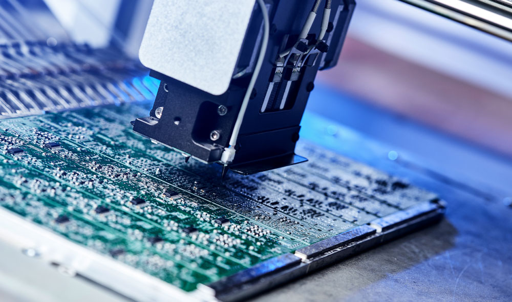
Precision in Motion
Our drilling machines are feats of engineering precision. They are computer-controlled marvels that select the appropriate drill size from a rack, ensuring accuracy before each use. These high-speed spindles rotate at an astonishing 180,000 revolutions per minute, creating clean hole walls that ensure secure connections. Dust and debris are our adversaries, but we have a master plan to conquer them.
A Clean Finish
To ensure our drilled holes are immaculate, we employ an advanced process that includes measurements, brushing, and high-pressure water jets. The Ishi high OPD bur takes 40 thickness measurements of each panel, optimizing the brush height for pristine hole cleanliness. Our mission is to create an impeccable foundation for what lies ahead.
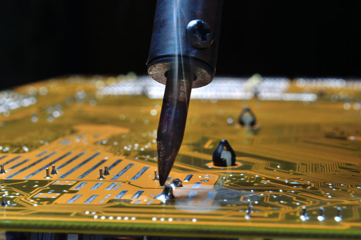
Copper Plating – Electrical Transformation
Have you ever wondered how copper gets into those tiny holes and traces? It’s all about electroplating. Panels are loaded onto flight bars, and a computer-controlled process prepares the copper surface for plating.
Etching Away the Unwanted
Now, it’s time to remove excess copper foil from the surface. We don’t want any copper where it shouldn’t be. A meticulously controlled alkaline solution dissolves away the exposed copper, inching down without straying sideways. This precision ensures that conductor widths match the design specifications perfectly.
Final Touch – Removing Tin and Copper
To reveal the pristine copper pattern, we strip away the thin tin coating that protected it during the plating process. This is the moment when the design you started with truly emerges, shining through.
Crafting Flexibility and Functionality – Solder Mask and Beyond
Solder Mask Application – Shielding the Copper Core
Flex circuit boards are all about adaptability and resilience, and that starts with the application of solder mask. This protective layer shields the copper surface, preventing solder shorting between components during assembly. Picture two high-production spray coating lines in action, gently showering the panel with a precise layer of solder mask. The advantage? Uniform thickness across the panel, thanks to a non-contact method of application.
The Art of Precision Printing
With the solder mask in place, we move on to the fine art of legend printing. Most flex circuit boards sport a component legend to guide the assembly process. Here’s where inkjet printers come into play, turning digital data into real-world legends directly on the board. The ink used in our inkjet legend printers is mil-certified and RoHS-compliant, ensuring an environmentally friendly process.

Quality Control: Where Flaws Meet Their Match
Before we consider our journey complete, every flex circuit board undergoes rigorous quality control. A team of sharp-eyed inspectors takes on this critical task. They meticulously inspect each board for cosmetic defects, ensuring a flawless finish. Beyond the surface, they measure the panel against mechanical drawings, checking hole diameters with a precision probe.
Sealing the Deal – Packaging and Shipping
As we near the end of our remarkable voyage, there’s one last step – sealing the deal. To protect your flex circuit boards from dirt and moisture, they are vacuum-sealed, bubble-wrapped, securely boxed, and prepared for shipping. Each board is treated like a treasure, with utmost care and attention to detail.
As we conclude this extraordinary journey from concept to flex circuit board reality, remember that every device you use is a testament to the precision and dedication that goes into manufacturing these technological marvels. Let’s explore in greater detail the manufacturing process of Flexible Printed Circuit Boards (PCBs).