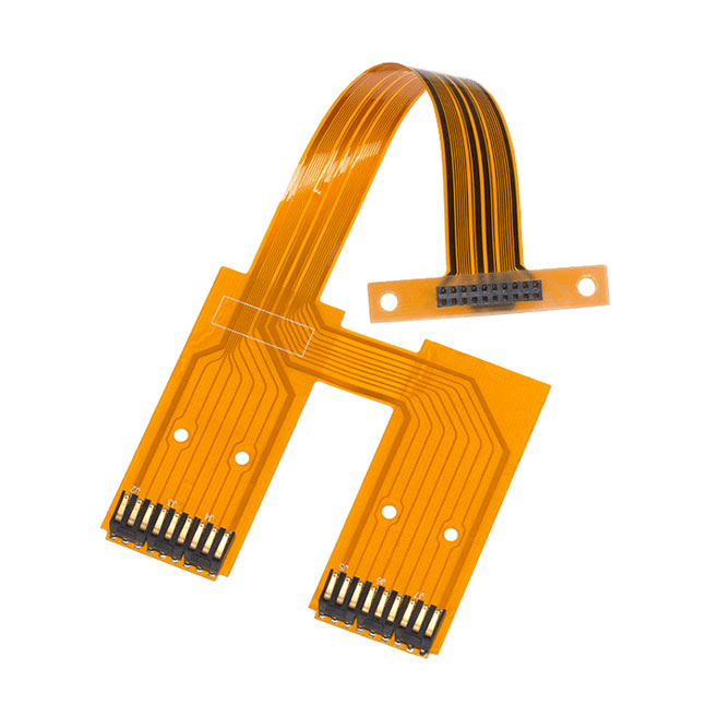
Flexible printed circuit boards (Flex PCBs) offer unique advantages for applications that require bendability, lightweight design, and space-saving layouts. The manufacturing process for flexible PCBs is distinct from that of traditional rigid PCBs.
Table of Contents
Overview of the flexible PCB manufacturing process
Material Selection
Flex PCBs are typically made from flexible materials like polyimide (PI) or polyester (PET). The choice of material depends on factors such as flexibility requirements, operating temperature, and cost. PI is commonly used for its high-temperature resistance.
Design and Layout
The design process for flexible PCBs begins with the creation of a flexible circuit layout using specialized PCB design software. Designers consider the specific application’s bending and flexing requirements, as well as component placement and routing.
Lamination
The chosen flexible material is coated with a layer of adhesive, which helps bond the layers together. Flex PCBs can consist of single, double, or multilayer configurations. The layers are then laminated together under heat and pressure.
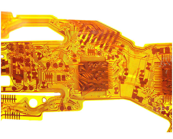
Etching
Just like in rigid PCB manufacturing, the copper layers on the flexible PCB are etched to create the desired circuit patterns. Etching removes excess copper, leaving behind the traces and pads.
Drilling
Holes are drilled into the flexible PCB to create vias for interconnecting different layers. Microvias, blind vias, and buried vias may be used, depending on the design requirements.
Plating
Copper is electroplated onto the walls of the drilled holes, creating conductive pathways for electrical connections between the layers. This process is crucial for maintaining signal integrity.
Solder Mask Application
A solder mask is applied to the flexible PCB to insulate the copper traces, protect against oxidation, and define soldering areas for components.
Surface Finish
Surface finishes like ENIG, OSP, or immersion tin are applied to enhance solderability and protect the exposed copper surfaces.
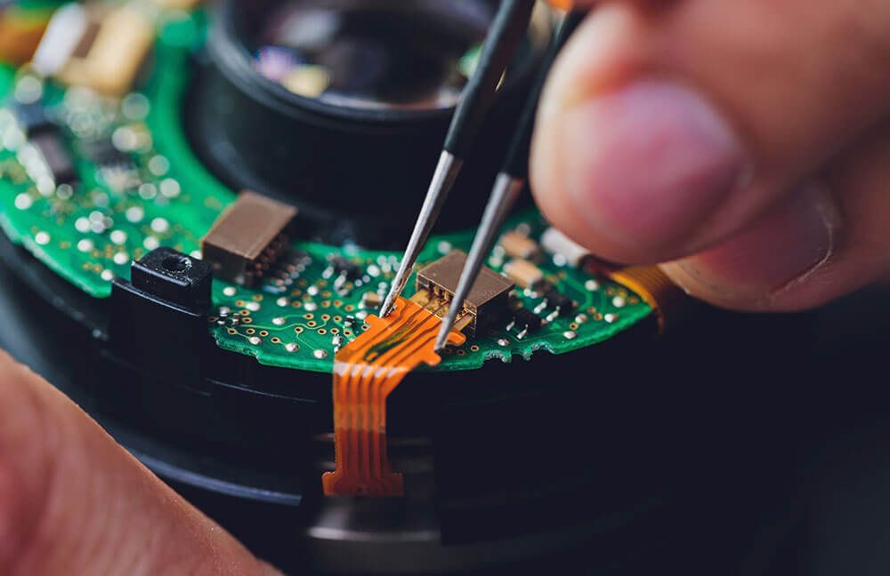
Component Assembly
Electronic components are placed and soldered onto the flexible PCB. This process may involve surface mount technology (SMT) for lightweight components and connectors designed for flex PCBs.
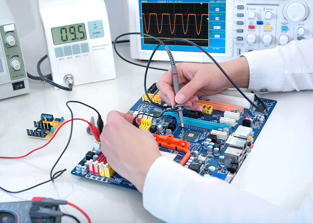
Testing
Flexible PCBs undergo electrical testing to ensure that the circuit functions correctly. This includes continuity checks and functional testing, particularly for flex PCBs used in critical applications.
Flexibility Testing
A critical step unique to flex PCB manufacturing is flexibility testing. The assembled flex PCB is subjected to bending, twisting, or flexing to ensure it meets the application’s requirements without damaging the circuit or solder joints.
Quality Control
Throughout the manufacturing process, strict quality control measures are implemented to identify and address any defects or issues. Here is a more detailed explanation of Quality Control in PCB Manufacturing.
Cutting and Trimming
After final testing and quality control checks, the flexible PCBs are cut and trimmed to the desired size and shape.
Difference between Flexible PCB manufacturing and traditional PCB manufacturing
Traditional PCB (printed circuit board) manufacturing and flexible PCB manufacturing are distinct processes tailored for different applications.
Design Considerations
Traditional PCBs emphasize fixed and rigid layouts with limited flexibility in mind. In contrast, flexible PCB designs are centered around achieving bendability, enabling these boards to conform to curved or irregular shapes. Designers of flexible PCBs must carefully assess factors such as bending radius and mechanical stability to ensure the board’s performance and reliability in applications that require flexibility.
Layers Configuration
Traditional PCBs are typically constructed with multiple rigid layers connected by through-hole vias. In contrast, flexible PCBs offer more versatility in their layer configuration, accommodating single, double, or multiple flexible layers. These flexible PCBs employ flexible interconnects and incorporate various via types, including microvias, blind vias, and buried vias, to enable intricate designs and enhance flexibility while maintaining electrical connectivity.
Material Handling
Traditional PCBs are relatively rigid and thus relatively easy to manage during the manufacturing and assembly processes. In contrast, the handling of flexible PCBs demands greater caution due to their inherent flexibility. To prevent any potential damage during production, specialized fixtures and tooling may be necessary for secure and precise manipulation of flexible PCBs.
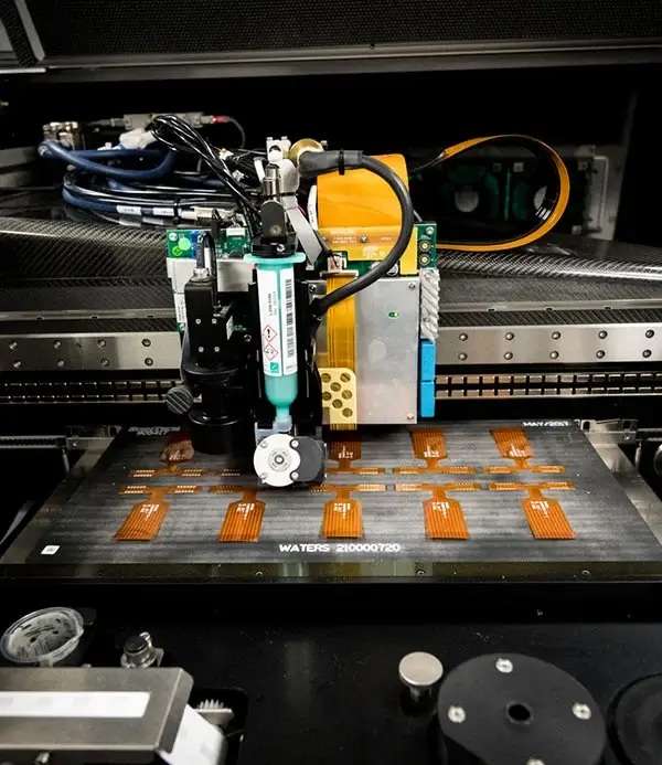
Manufacturing equipment
Traditional PCBs is meticulously tailored for processing rigid boards, encompassing drilling, etching, and plating equipment optimized for such applications. Conversely, the production of flexible PCBs necessitates specialized machinery equipped to handle and process flexible materials adeptly. This specialized equipment often includes precision laser drilling technology essential for creating microvias in flexible PCBs, reflecting the distinctive requirements of the flexible PCB manufacturing process.
Flexible PCB manufacturing demands precision, attention to detail, and specialized equipment to ensure the reliability of the final product, especially when it will be subject to repeated bending and flexing. Flex PCBs find applications in industries such as aerospace, medical devices, automotive, and consumer electronics, where their unique properties provide a competitive edge in design and functionality.