Table of Contents
Core Definition and Functions of Stamp Holes
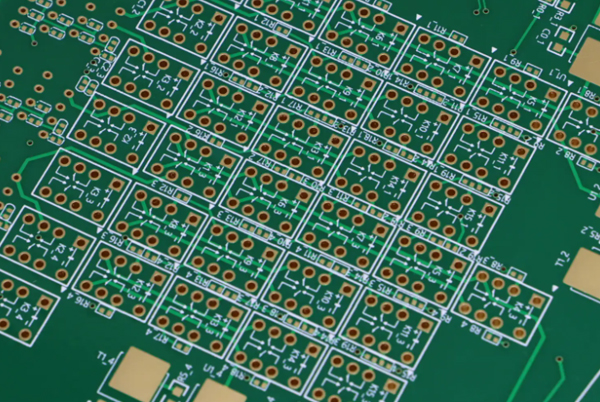
PCB stamp holes (also known as breakaway tabs or panelization holes) are arrays of small through-holes designed along PCB edges or panel connections, named for their resemblance to perforated stamp edges. This structure plays a critical role in electronics manufacturing:
- Mechanical Connection and Separability
- Uses micro through-hole arrays (typically 0.5mm diameter, grouped in sets of 5-8) for temporary PCB interconnections
- Allows post-production separation via mechanical breaking without specialized milling equipment
- Particularly suited for irregularly shaped PCBs (e.g., circular, non-linear outlines)
- Electrical Connectivity
- Serves as a power/signal transmission channel in modular designs
- Requires impedance matching considerations for high-frequency applications
- Manufacturing Advantages
- Enhances SMT assembly efficiency by enabling small PCBs to traverse production lines as arrays
- Reduces processing costs compared to V-CUT for complex board separation
Technical Parameters of Stamp Holes
| Parameter Category | Standard Value | Tolerance | Key Considerations |
|---|---|---|---|
| Hole Diameter | 0.5mm | ±0.05mm | Must exceed 1/3 board thickness |
| Hole Pitch | 0.76mm | ≥0.3mm | Short-circuit prevention |
| Row Spacing | 3.3mm | – | Mechanical strength balance |
| Edge Margin | 1.0mm | ≥0.5mm | Burr prevention |
Special Design Rules:
- High-frequency circuits: Requires shielded ground holes
- High-density boards: Recommends staggered dual-row layouts
- Rigid-flex boards: Requires reinforced zones
Comparative Analysis with V-CUT Technology
V-CUT Characteristics
- Applications: Straight-line board separation, standard rectangular PCBs
- Advantages:
- ~30% cost reduction (eliminates additional drilling steps)
- Post-separation edge flatness within ±0.1mm
- Ideal for high-volume standardized production
Key Benefits of Stamp Holes
- Geometric Adaptability: Accommodates curved separation paths
- Mechanical Performance:
- 40% higher bending resistance than V-CUT
- Enables smaller inter-board spacing (minimum 1.5mm)
- Assembly Convenience:
- Provides 25% greater adhesive surface area
- Supports modular disassembly/reconfiguration
IPC-Compliant Design Standards
Preferred Design (IPC-7351 Class A)
- Trace-to-hole clearance ≥1mm
- Copper retention rate >80%
- Teardrop pad transitions
High-Risk Designs (Class C)
- Trace-to-edge spacing <0.5mm
- Presence of right-angle trace transitions
- Missing solder mask dams
Critical Engineering Practices
- Layout Prohibitions:
- No stamp holes within 3mm of BGA packages
- Avoid parallel high-speed signal routing through hole arrays
- Reliability Enhancements:
- Add 0.3mm process margins as buffer zones
- Implement copper mesh reinforcement in high-stress areas
- Manufacturability Checks:
- Ensure minimum hole diameter ≥1/3 board thickness
- Verify whole wall copper thickness ≥18μm
Typical Application Scenarios
- Wearable Devices:
- Enables rigid-flex zone transitions via stamp holes
- Example: Smartwatch heart rate module connections
- Industrial Control Systems:
- Provides mechanical alignment and electrical interconnection for stacked boards
- Stress-relief structures in vibration-resistant designs
- Automotive Electronics:
- Modular service interfaces for ECU control boards
- Redundant connection solutions for high-vibration environments