Table of Contents
What is PCB?
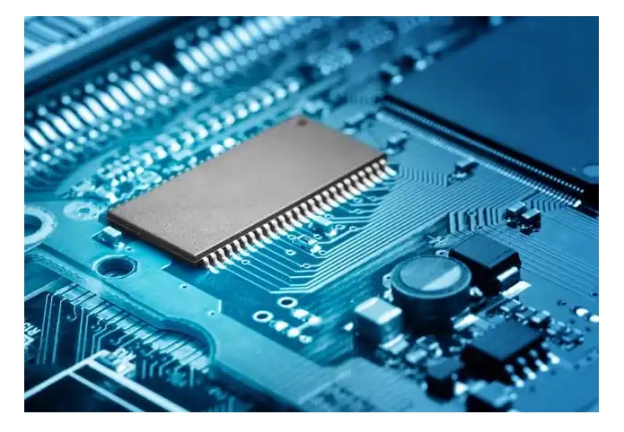
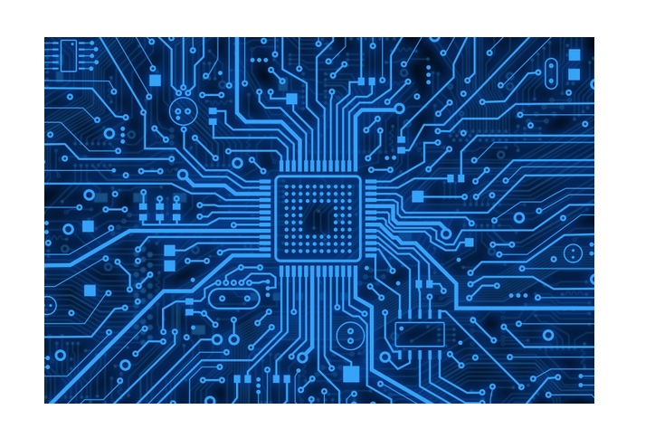
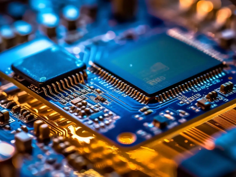
A Printed Circuit Board(PCB) is the basic component of modern electronic equipment, like the skeleton of the human body supporting all electronic components. It consists of an insulated substrate, copper foil lines, and various protective layers, manufactured through the printing and etching process. It not only supports various electronic components but is also responsible for signaling between them.
From our daily use of cell phones, computers, home appliances, to cars, medical equipment, and even space satellites, almost all electrically charged products can not be separated from the PCB. Imagine if there is no PCB, our electronic devices will need a lot of messy wire connections, not only is the volume huge, but the reliability is extremely low, our smartphones may need a suitcase as big as to fit all the connecting wires.
The Evolution of PCB
PCB Technology Development Timeline
1925
- Concept Sprouted: American Charles Ducas printed circuit patterns on insulated substrates for the first time.
1936
- First Practical Application: Austrian Paul Eisler used PCBs in radios.
1940s–1950s
- Military & Commercialization: World War II accelerated PCB development for military use.
- Mainstream Technology: Single-panel PCBs became dominant.
1960s
- Space Race Boost: The Apollo program drove PCB advancements.
- Mass Production: Double-sided boards entered large-scale production.
1970s
- Rise of Multilayer PCBs: More complex designs enabled higher circuit density.
1980s
- Surface Mount Technology (SMT): Replaced traditional through-hole insertion.
- PC Revolution: Surging demand for PCBs due to personal computers.
1990s
- Advanced Packaging: Ball Grid Array (BGA) technology emerged.
21st Century
- High-Density & Flexibility:
- HDI (High-Density Interconnect): Enabled finer circuits.
- Flexible PCBs: Expanded applications in wearables and compact devices.
Today’s Precision
- Line Width: As fine as 0.05mm (half a human hair’s diameter).
- Multilayer Boards: Up to 30+ layers.
- Micro-Vias: Through-hole diameters as small as 0.1mm.
Common types of PCB
1. Distinguished by structure
Rigid PCB
Characteristics: strong and durable, as solid as the foundation of the building
Advantage: Affordable, mature production technology
Used in fixed electronic products that do not require bending, such as desktop computer motherboards, TV control boards, and air conditioners.
Flexible PCB
Characteristics: thin and flexible, can be bent and folded
Advantage: space saving, adapts to special shapes
Applied to products that need to be bent or have space constraints, such as smartphone internal connections, smartwatch circuits, and wearable devices.
Rigid-flexible board
Characteristics: both the solidity of the rigid area and the flexibility of the flexible area
Advantage: Integrated design for higher reliability
Applied to products with high requirements for space and reliability, such as high-end camera modules, UAV flight control systems, and medical endoscopes.
2. Distinguish by layers
Single panel
Characteristics: only one side has lines, and the simplest structure.
Advantage: lowest cost, fastest production
Apply to simple low-end electronic products, such as: simple electronic toys, LED light control board, basic electronic clocks, and watches.
Double-sided panel
Features: wiring on both front and back, connected through small holes
Advantage: affordable and functional enough
Applied to most common electronic products, such as: smart home controller, common home appliance circuit, and automobile basic electronic module.
Multi-layer board
Characteristics: like a sandwich with multiple layers of circuitry
Advantage: large wiring space, strong anti-interference
Applied to complex functionality of professional equipment, such as: computer motherboards, industrial control equipment, and communication base stations.
HDI board
Characteristics: extremely fine lines, high density
Advantage: small size, strong performance
Used in the pursuit of thin and light high-end electronic products, such as smartphone motherboards, ultra-thin notebook computers, and high-end digital cameras.
3. How to choose the right type of PCB?
- Single/double-sided boards for limited budgets.
- Need to bend the selection of flexible boards
- Complex function choosesa multilayer board
- The pursuit of a thin and light choice of HDI board
The basic components of a PCB
A complete PCB is like a well-designed multi-layer cake:
1.Base layer
Commonly used materials: FR4 glass fiber plate (similar to reinforced plastic), ordinary electronic products choose FR4 is enough, special needs can be considered metal substrate or ceramic substrate.
Role: to provide solid support, insulation, non-conductive to prevent short-circuit, high temperature welding without deformation.
2.Conductive layer (copper foil line)
Production process: the formation of precision circuits through chemical etching, the wider the line, the greater the current that can pass.
Role: excellent conductivity (second only to silver), the thickness is usually only 1/3 of the diameter of the hairline, and the line width can be as small as 0.1 mm.
3.Soldermask
Common colors: green (90%), also blue/red/black, etc. Green became mainstream because the military initially specified the standard color.
Role: to prevent short-circuiting when soldering, to protect copper wires from corrosion, to provide a protective layer of insulation.
4.Character layer
Circuit board instructions: component number (such as R1, C2), polarity marking (+ / – pole), the manufacturer’s logo, and production information.
Role: to facilitate assembly and maintenance, provide safety warnings, and record product information.
Surface treatment
Common processes: tin spraying (most economical), gold immersion (high reliability), gold plating (high-end products).
Function: Prevent oxidation of copper foil, improve soldering performance, and extend the life of the board.
The role of PCB
1. Mechanical support
PCB for all kinds of electronic components to provide a solid mounting platform, can firmly fix chips, resistors, capacitors, and other components, to maintain the precise relative position between the components, as well as to withstand the vibration and impact of daily use.
Typical example: smartphone motherboards should be able to withstand hundreds of drop tests.
2.Electrical Connections
The copper-clad lines on the PCB are like a city road system, connecting hundreds of components to ensure efficient signal transmission, with a clear division of labor between different lines (power transmission, data communication, etc.). The wiring of a modern cell phone PCB can be several kilometers long if unfolded.
3.Insulation protection
PCB, through careful design, you can prevent circuit confusion, the reasonable layout can prevent the signal from interfering with each other (crosstalk), and soldermask can effectively isolate adjacent lines to avoid short circuits. For high-voltage hazardous areas, but also need to have a special is also needed.
Typical case: home appliance control boards to ensure the safe use for more than ten years
Advantages of PCBs over manual wiring
1.Volume and weight advantages
Greatly save space, modern PCBs can originally need the size of a shoe box of manual wiring condensed to the size of a credit card, PCB lines instead of hundreds of independent wires, greatly reducing the weight. On this basis, it can support the design of thinner and more fashionable electronic products.
2.Reliability and consistency advantages
PCB failure rate reduced to only 1/100 of the manual wiring, the machine set up the program, mass production, each circuit board is as accurate as a replica, and the durability is extremely strong, even if it is subjected to more than 1,000 times of insertion and removal test, there is not too much impact, so that the electronic products are more durable, the maintenance rate has dropped dramatically, and cost savings.
3.Production efficiency advantages
In terms of production speed, 1 set of automatic mounter can complete the accurate installation of more than 50,000 components per hour, and the cost is only 1/10 of the handmade, or even less, after the completion of each process, it will be automated through a variety of equipment testing, to ensure that each piece of circuit board is flawless.
Core Manufacturing Process
1.Graphics Transfer
The essence of the process: the circuit diagram designed by the engineer is precisely “copied” onto the copper foil.
Technology highlights: similar to photo printing, but a hundred times finer, the use of photolithography technology, the accuracy can reach the micron level, determining the precision of the final circuit.
2.Etching Process
Working Principle: Dissolve unwanted copper with a special potion.
Process Points: Remove the excess copper foil with a special potion and keep the designed circuit.
3.Laminating technology
Process Characteristics: Ensure the layers are perfectly aligned and then bond the multilayer materials under high temperature and pressure.
Application value: Realize complex multilayer circuits and improve product reliability.
4.Drilling technology
Technology evolution: mechanical drilling (0.2mm), laser drilling (0.02mm)
Process breakthrough: extremely high positional accuracy, hundreds of holes can be drilled in an area of the size of a fingernail, and to ensure that the hole wall is smooth and burr-free.
5.Surface treatment
Common processes: spray tin (the most economical), immersion gold (high performance), gold-plated (high-end products).
Core role: to ensure good weldability, to protect the copper layer from rust, to extend the product life.
Application Areas
Consumer Electronics
PCBs in smartphones are works of art, using HDI technology and arbitrary layer interconnection design to realize complex functions in a space the size of a fingernail cap. Smart home devices pay more attention to PCB cost control and reliability.
Automotive Electronics Applications
Engine Control Unit (ECU), in-vehicle infotainment systems, ADAS advanced driver assistance, electric vehicle battery management systems, etc.
Industrial Grade PCB
Wide temperature working capability, super durability (anti-vibration, anti-corrosion), long-term supply stability (more than 10 years).
Medical Equipment PCB
Ultra-high reliability (life-support equipment), low-noise design (precision testing instruments), etc.
PCB future development trend
As electronic products continue to miniaturize and intelligent, PCB technology also continues to innovate, the need for finer lines to adapt to micro-components, higher density unit area to accommodate more functionality, in line with environmental standards such as RoHS, more intelligent design, integrated sensors, and other new features.
From the initial single-layer boards to today’s high-density interconnect boards, PCB technology has always driven the development of the electronics industry. PCB will continue to play an irreplaceable role in the era of intelligence. Whether you are an ordinary consumer or an engineer, understanding the basics of PCBs will help you to better use and maintain electronic devices.