In the electronics manufacturing industry, PCB panelization design is a crucial step that connects design and production. An excellent panel design can significantly improve production efficiency and reduce costs, while a poor design may lead to production bottlenecks and quality issues. This article will explore all aspects of PCB panelization design to help you master this essential skill.
Table of Contents
What is PCB Panelization Design and Why is it So Important?
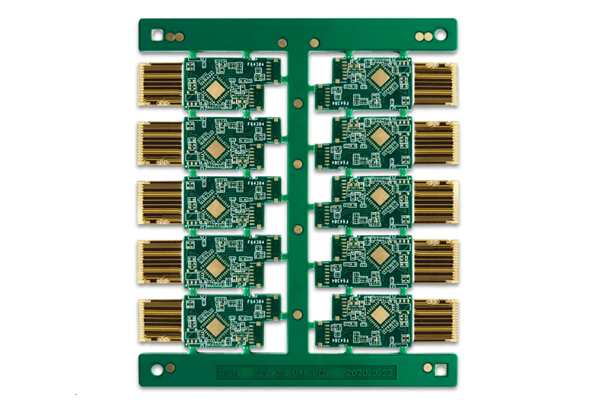
PCB panelization design refers to the strategic arrangement of multiple small PCB boards on a larger production panel. Imagine printing multiple photos together on one sheet rather than printing each photo separately – this dramatically improves production efficiency.
The importance of panelization design manifests in three core aspects:
- Improved Production Efficiency: SMT placement machines can process tens of thousands of components per hour, but frequent small board changes drastically reduce machine utilization. Panelization allows machines to process multiple PCBs at once, minimizing downtime. Our experience shows that proper panel design can improve SMT line efficiency by over 30%.
- Cost Control: PCB production always generates material waste. Good panel design maximizes material utilization. We helped one client optimize their panel layout to increase material utilization from 78% to 92%, saving ¥150,000 annually in material costs alone.
- Quality Consistency: All boards on the same panel experience identical production conditions, resulting in better consistency compared to individually produced boards. This is particularly crucial for reflow soldering processes where temperature profile consistency is vital for soldering quality.
Key Elements of PCB Panelization Design
1. The Golden Rules of Panel Size
Selecting panel size isn’t arbitrary – multiple factors must be considered:
- Equipment Limitations: Different SMT equipment has specific maximum and minimum panel size requirements. Typically, optimal panel sizes range between 250×200mm to 300×250mm. We recommend confirming equipment specifications with your SMT supplier before design.
- Operational Convenience: Oversized panels may cause handling difficulties and increase production breakage risks. We encountered a case where a client designed 400×350mm panels that frequently jammed during conveyance, requiring redesign.
- Material Utilization: Ideally, panel sizes should divide evenly into standard copper-clad laminate sizes (like 457×610mm) to minimize waste. Panel size calculation tools can help find optimal solutions.
Practical Tip: Create a panel size template library documenting historically successful sizes as starting points for new projects.
2. The Art of Panel Spacing and Connection Methods
Panel spacing and connection methods directly affect subsequent depaneling processes and quality:
V-Cut Design Essentials:
- Suitable for straight-line separation of regular shapes
- Remaining V-groove thickness should be 1/3 of board thickness (typically 0.5mm)
- The groove angle is usually 30 or 45 degrees
- Maintain at least 2mm clearance between components and V-cut lines
Tab Routing Design Essentials:
- Suitable for irregular shapes or sensitive component areas
- Typical bridge width: 3-5mm
- Place connection points every 10-15cm
- Recommended drill diameter: 0.8-1.0mm
Breakaway Tab Design Essentials:
- Suitable for ultra-thin or flexible boards
- Hole diameter: 0.5-0.8mm
- Hole spacing: 1-1.5mm
- Must consider burr treatment solutions
Experience Sharing: For designs with sensitive components like BGAs or QFNs, we recommend tab routing over V-Cut because depaneling stress may cause solder joint cracks.
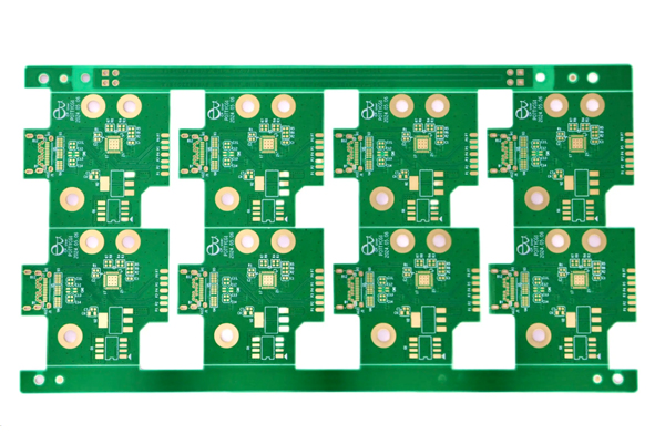
3. The Principle of Component Orientation Consistency
Component orientation consistency significantly impacts placement efficiency:
- Best Practice: Maintain uniform component orientation across all boards on a panel. In one case study, unifying component orientation increased placement speed from 35,000 to 42,000 points per hour.
- Polarized Components: Ensure consistent orientation for diodes, electrolytic capacitors, etc., to prevent manual inspection errors.
- High-Density Area Planning: Distribute high-density component areas evenly across panels to prevent localized heat concentration.
Practical Tip: Use panel simulation software to model placement head movement paths and optimize component layout orientation.
4. Error-Proofing Techniques for Pad and Via Design
Improper pad and via design may cause soldering defects:
- Edge Protection: Keep all pads at least 1mm from depaneling edges, especially near V-cut lines.
- Via Treatment:
- Plated through-holes: Recommend solder mask coverage
- Vias: Diameters <0.3mm can use the plugging process
- BGA areas: Must use the plugging process
- Test Point Design:
- Minimum one test point per net
- Test point diameter ≥0.8mm
- Test point spacing ≥2.54mm
Case Study: A client experienced 5% pad detachment after depaneling because pads were only 0.3mm from V-cut lines. Increasing this to 1.2mm completely resolved the issue.
Advanced PCB Panelization Techniques
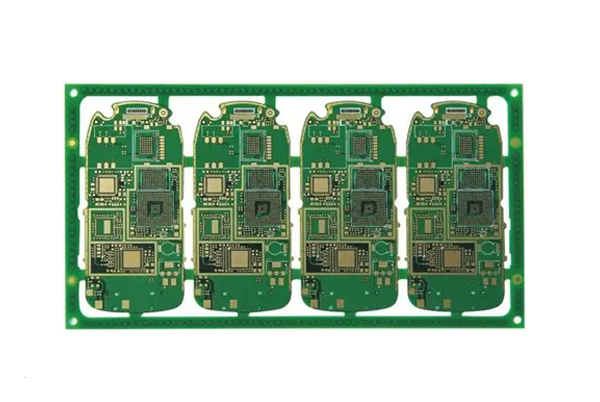
1. Mixed Panel Strategy
Mixed panelization arranges different PCB designs on one production panel. This strategy can:
- Improve small-batch production efficiency
- Reduce changeover time
- Balance production scheduling
Implementation Points:
- Ensure all PCBs have identical thickness
- Copper weight variation ≤1oz
- Identical surface finish processes
- Compatible reflow profiles
Success Story: We helped a smart home client panelize 5 different PCBs together, improving small-batch production efficiency by 60%.
2. Thermal Balance Design
Thermal balance is crucial during reflow soldering:
- Component Distribution: Distribute high-power components evenly to prevent localized overheating
- Copper Balance: Design large copper areas symmetrically
- Thermal Mass Consideration: Alternate dense and sparse component areas
Practical Method: Use thermal simulation software to analyze panel heat distribution, adjusting layouts until temperature variation is <5℃.
3. Design for Testability and Manufacturability (DFM/DFT)
Excellent panel design must consider testing and manufacturing:
- Test Point Layout: Ensure test probes can access all board test points simultaneously
- Depaneling Marks: Clear markings reduce depaneling errors
- Tooling Edge Design: Typically requires 5mm edges for clamping and positioning
Pro Tip: Adding fiducial marks aids SMT placement and improves depaneling accuracy. Each board should have at least 2 diagonal fiducials.
Common PCB Panelization Issues and Solutions
Issue 1: Burrs or Copper Foil Lifting After Depaneling
Solutions:
- Verify V-cut depth (should be 2/3 board thickness)
- Consider switching to tab routing
- Add copper protection strips along the depaneling edges
- Implement edge grinding post-depaneling
Issue 2: Panel Warping During Reflow
Solutions:
- Review panel thermal balance design
- Increase panel symmetry
- Consider higher Tg substrate materials
- Optimize the reflow profile with slower ramp rates
Issue 3: Determining the Optimal Number of Boards Per Panel
Solutions:
- Consider SMT equipment capacity limits
- Balance material utilization and handling convenience
- Conduct DOE testing with different board counts
- Typical recommendation: 4-12 boards per panel
Issue 4: Ensuring Consistent Soldering Quality in Mixed Panels
Solutions:
- Select designs with similar thermal characteristics
- Verify temperature distribution with thermal simulation
- Adjust component layout for balanced thermal mass
- Consider segmented reflow processes
Issue 5: Panel Design Impact on ICT Testing
Solutions:
- Ensure test points survive depaneling
- Plan for pre-post-depaneling test strategies
- Design adequate test point spacing (≥2.54mm)
- Mark critical test point locations
Issue 6: Reducing Stress Concentration in Panel Designs
Solutions:
- Avoid placing sensitive components near bridges
- Use rounded corners instead of sharp corners
- Consider stress simulation analysis
- Optimize bridge quantity and placement
Conclusion and Best Practice Recommendations
Excellent PCB panelization design combines art and science. Based on our discussion, we recommend these best practices:
- Plan Early: Consider panel requirements during PCB layout, not as an afterthought.
- Collaborate with Suppliers: Work closely with SMT and PCB manufacturers to understand their capabilities and limitations.
- Standardize: Develop internal panel design guidelines to improve consistency.
- Continuous Improvement: Collect production feedback to refine panel designs.
- Leverage Tools: Use specialized panel design and simulation software to reduce trial-and-error costs.
Remember, a good panel design should resemble a well-orchestrated symphony – every element in perfect harmony, working together to create an efficient, cost-effective production process.
Recommended Reading
High Speed PCb Design
PCB Design and Manufacturing
Common Problems and Solutions in PCB Design