Signal integrity is no longer a concern only for RF engineers.
In modern high-speed digital designs, even standard multilayer PCBs can experience signal degradation if manufacturing variables are not tightly controlled.
Many engineers focus heavily on layout and simulation—but overlook how the PCB manufacturing process directly impacts real-world electrical performance.
In this guide, TOPFAST, a professional PCB manufacturer, explains how fabrication variables influence signal integrity and what designers can do to minimize risk.
Table of Contents
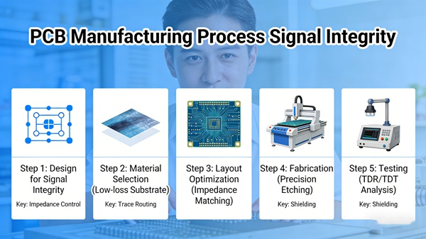
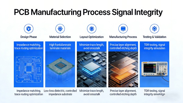
Why Manufacturing Matters for Signal Integrity
Signal integrity depends on:
- Controlled impedance
- Consistent dielectric thickness
- Stable copper geometry
- Precise layer alignment
These parameters are all influenced by fabrication processes such as lamination, etching, and plating.
If you are unfamiliar with the full fabrication flow, we recommend reviewing our
PCB manufacturing process guide
Understanding the process is the first step toward understanding electrical variation.
1. Trace Width Variation and Impedance Control
During etching, copper traces rarely maintain their exact designed width.
Minor over-etching can reduce trace width, increasing impedance.
Even small variations can affect:
- High-speed digital signals
- Differential pair matching
- RF transmission lines
Designers should consider realistic PCB manufacturing tolerances when defining impedance structures.
Ignoring tolerances often results in impedance mismatch during real production.
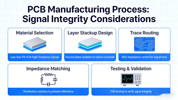
2. Dielectric Thickness Variation
PCB impedance is heavily influenced by dielectric thickness between signal layers and reference planes.
During lamination:
- Resin flow may cause thickness variation
- Press temperature and pressure impact uniformity
- Material Tg affects dimensional stability
Even controlled processes have measurable variation.
Professional manufacturers manage this through stack-up optimization and material selection.
3. Copper Roughness and Signal Loss
Copper surface roughness increases insertion loss, especially at high frequencies.
As frequency increases:
- Skin effect intensifies
- Rough copper causes additional attenuation
Selecting appropriate copper types (e.g., low-profile copper) can significantly improve high-speed performance.
Manufacturers that understand signal integrity will recommend suitable material options during DFM review.
4. Layer Misregistration
Misalignment between signal and reference layers can alter impedance and coupling behavior.
This can affect:
- Crosstalk performance
- Return path continuity
- EMI performance
Layer alignment precision is controlled during lamination and imaging processes.
Poor process control increases electrical unpredictability.
5. Via Quality and High-Speed Performance
Vias introduce impedance discontinuities.
Manufacturing factors affecting vias include:
- Plating thickness
- Hole wall quality
- Drill accuracy
Defects such as voids or insufficient plating (see common PCB manufacturing defects) can increase resistance and degrade high-speed signals.
Proper via design, combined with stable plating processes, is essential for reliable signal transmission.
Signal Integrity Risks in Standard vs HDI PCBs
Standard Multilayer PCBs
- Moderate impedance sensitivity
- More forgiving of small variations
HDI / High-Speed PCBs
- Tight impedance requirements
- Sensitive to dielectric variation
- Sensitive to copper roughness
As PCB density increases, manufacturing precision becomes more critical.
How TOPFAST Controls Signal Integrity Variables
As a professional PCB manufacturer, TOPFAST supports high-speed designs through:
- Controlled impedance stack-up design
- Process capability validation
- Statistical thickness monitoring
- Impedance test coupon verification
- Strict quality control throughout fabrication
(Internal link to: /pcb-quality-control/)
This ensures electrical performance matches simulation expectations.
Design Recommendations for Engineers
To reduce signal integrity risk during fabrication:
- Design impedance structures with realistic tolerances
- Communicate critical nets clearly
- Use manufacturer-reviewed stack-ups
- Avoid unnecessary ultra-tight constraints
- Perform impedance coupon verification
Collaboration between design and manufacturing teams significantly improves high-speed performance consistency.
PCB Manufacturing Process FAQ
A: Yes. Variations in trace width, dielectric thickness, and copper roughness directly influence impedance and signal loss.
A: No process is perfect, but tight process control and impedance testing significantly reduce variation.
A: Only when required by performance. Over-specification increases cost without always improving performance.
A: Impedance test coupons and electrical testing during fabrication are standard verification methods.
Conclusion
Signal integrity does not depend solely on design software and simulation tools.
It is equally dependent on real-world manufacturing control.
Understanding how PCB fabrication variables influence impedance, loss, and high-speed behavior allows engineers to design smarter, reduce risk, and improve product reliability.
With controlled impedance capability and strict process management, TOPFAST helps ensure your PCB performs electrically exactly as designed.