Printed Circuit Board (PCB) manufacturing is the foundation of all electronic products.
The quality of a PCB directly affects signal integrity, product reliability, and long-term performance.
In this guide, TOPFAST, a professional PCB manufacturer, explains the complete PCB manufacturing process step by step—from design review to final inspection—based on real factory practices used in prototype and mass production.
Whether you are an engineer, purchaser, or product manager, understanding how PCBs are manufactured helps you make better design and sourcing decisions.
Table of Contents
Overview of the PCB Manufacturing Process
PCB manufacturing is a multi-stage process that transforms raw laminate materials into a fully functional bare circuit board.
Key Stages of PCB Fabrication
- PCB design review (DFM & DRC)
- Raw material preparation
- Inner layer imaging and etching
- Lamination and layer alignment
- Drilling and via formation
- Copper plating
- Outer layer imaging
- Solder mask application
- Surface finish
- Electrical testing and final inspection
Each step plays a critical role in ensuring electrical performance, mechanical stability, and manufacturing yield.
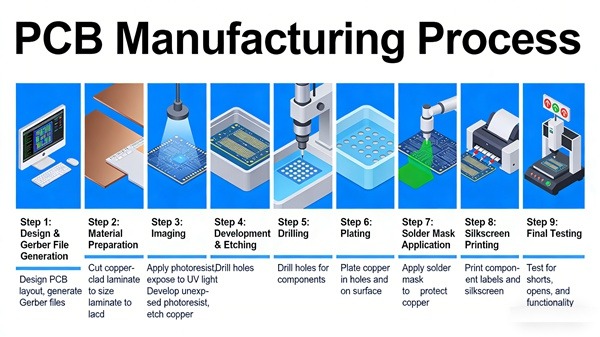
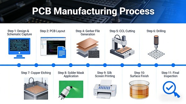
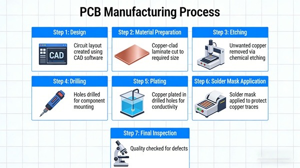
Step 1: PCB Design Review (DFM & DRC)
Before production begins, PCB design files must pass a Design for Manufacturability (DFM) and Design Rule Check (DRC).
This step ensures that the design can be manufactured reliably and cost-effectively.
What Is Checked During DFM?
- Trace width and spacing
- Annular ring size
- Drill-to-copper clearance
- Solder mask openings
- Impedance control requirements
- Panelization efficiency
At TOPFAST, experienced engineers review every PCB file and provide optimization suggestions when needed, helping customers avoid production delays and unexpected costs.
Step 2: Raw Material Preparation
Once the design is approved, the manufacturing process begins with material preparation.
Common PCB Base Materials
- FR-4 (standard and high-Tg)
- High-frequency laminates (Rogers, Taconic, etc.)
- Aluminum substrate (for thermal management)
- Polyimide (for flexible PCBs)
Material selection affects electrical performance, heat dissipation, mechanical strength, and overall cost. Choosing the right laminate is essential for long-term reliability.
Step 3: Inner Layer Imaging and Etching
For multilayer PCBs, inner copper layers are processed first.
Inner Layer Manufacturing Process
- Dry film lamination
- UV exposure with artwork
- Developing to reveal the copper pattern
- Chemical etching to remove excess copper
- Stripping of photoresist
Why Inner Layer Accuracy Matters
- Ensures correct impedance
- Maintains signal integrity
- Prevents layer misalignment
- Improves yield in multilayer boards
Precision at this stage determines the electrical performance of the final PCB.
Step 4: Lamination and Layer Alignment
After the inner layers are completed, they are stacked together with prepreg and laminated under controlled pressure and temperature.
Lamination is one of the most critical steps in multilayer PCB manufacturing.
Common Lamination Defects
- Layer misregistration
- Resin voids
- Delamination
- Thickness inconsistency
As a professional PCB manufacturer, TOPFAST applies strict lamination control to ensure stable layer alignment and mechanical integrity.
Step 5: Drilling and Via Formation
Drilling creates electrical connections between PCB layers.
Types of PCB Drilling
- Mechanical drilling
- Laser drilling (microvias)
- Blind vias
- Buried vias
Drill accuracy directly affects reliability and plating quality, especially for HDI and high-density designs.
Step 6: Copper Plating Process
After drilling, the holes are plated with copper to form conductive vias.
Copper Plating Includes
- Electroless copper deposition
- Electrolytic copper plating
Why Plating Thickness Matters
- Improves the current carrying capacity
- Enhances via reliability
- Extends product lifespan
Insufficient or uneven plating can cause open circuits and premature failure.
Step 7: Outer Layer Imaging
Outer layer imaging defines the final circuit pattern on the top and bottom layers.
This step requires high precision to support:
- Fine-pitch components
- BGA and QFN packages
- High-speed signal routing
Accurate imaging of the outer layer ensures proper soldering and electrical performance.
Step 8: Solder Mask Application
Solder mask is applied to protect copper traces and prevent solder bridges during assembly.
Functions of Solder Mask
- Electrical insulation
- Short-circuit prevention
- Environmental protection
- Improved appearance
Common colors include green, black, blue, red, and white, depending on application needs.
Step 9: Surface Finish Options
Surface finish protects exposed copper and ensures solderability.
Common PCB Surface Finishes
| Surface Finish | Advantages | Typical Applications |
|---|---|---|
| HASL | Low cost, durable | Consumer electronics |
| ENIG | Flat surface, long shelf life | BGA, fine-pitch ICs |
| OSP | Eco-friendly, low cost | High-volume production |
| ENEPIG | Excellent reliability | Advanced semiconductor packages |
Choosing the right surface finish balances cost, reliability, and assembly requirements.
Step 10: Electrical Testing and Final Inspection
Before shipment, every PCB must pass electrical and visual inspections.
Quality Control at TOPFAST
- Flying probe electrical test
- Automated Optical Inspection (AOI)
- X-ray inspection (for HDI boards)
- IPC Class 2 / Class 3 compliance
Strict quality control ensures that every PCB meets design specifications and reliability standards.
How the PCB Manufacturing Process Affects Cost
Multiple factors influence PCB manufacturing cost:
- Number of layers
- Material type
- Board thickness
- Surface finish
- Trace width and spacing
- Order quantity
Understanding these factors helps engineers optimize designs and reduce total project cost.
PCB Manufacturing vs PCB Assembly (Fabrication vs PCBA)
It is important to distinguish between PCB manufacturing and PCB assembly.
- PCB Manufacturing: Producing the bare circuit board
- PCB Assembly (PCBA): Mounting and soldering components onto the PCB
TOPFAST provides both services, helping customers streamline their supply chain from bare board to fully assembled PCBA.
Why Choose TOPFAST for PCB Manufacturing
- In-house manufacturing capabilities
- Professional DFM engineering support
- Fast prototype and mass production
- Strict quality control
- Global shipping and technical support
With extensive manufacturing experience, TOPFAST supports customers from concept to production with confidence.
Conclusion
Understanding the PCB manufacturing process helps engineers improve design quality, control cost, and ensure long-term reliability.
By combining advanced manufacturing technology with strict quality control, TOPFAST, a professional PCB manufacturer, delivers high-quality PCBs from prototype to mass production.
PCB Manufacturing FAQ
A: Prototype PCBs typically take 3–7 working days, while mass production depends on complexity and order volume.
A: Gerber files, drill files, stack-up details, and impedance requirements are commonly required.
A: This depends on PCB complexity and material, but advanced manufacturers can support very fine geometries.
A: Yes. TOPFAST supports both prototype and volume production with flexible order quantities.