When engineers or purchasing teams request a PCB quote, one of the most common questions is:
“Why does this board cost this much?”
PCB fabrication cost is not a single number—it is the result of multiple manufacturing steps, material choices, and process requirements.
This guide explains how PCB manufacturing cost is structured, which steps contribute the most, and how design decisions influence total production price.
Table of Contents
What Determines PCB Manufacturing Cost?
PCB cost is influenced by four main factors:
- Board structure (layer count, stack-up)
- Material selection
- Process complexity
- Required tolerances and quality level
To understand cost properly, it helps to look at the actual PCB manufacturing process step by step.
Each stage adds measurable cost depending on complexity and precision requirements.
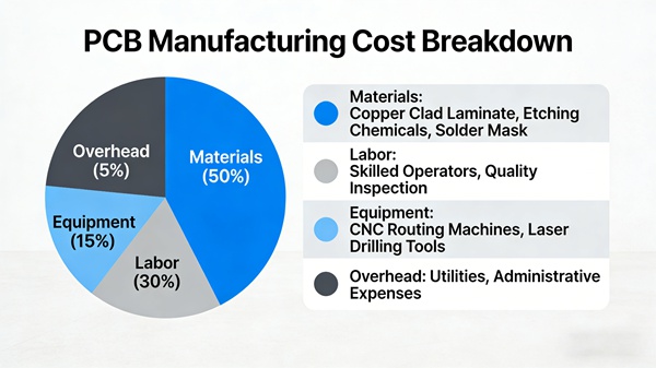
1. Raw Material Cost
Material is the foundation of fabrication cost.
Key components include:
- Copper-clad laminate (FR4, high-Tg, Rogers, etc.)
- Prepreg sheets
- Copper foil thickness
- Surface finish chemicals
Higher Tg materials, low-loss laminates, or specialty substrates significantly increase cost compared to standard FR4.
Material choice alone can account for a large portion of the total PCB price.
2. Layer Count and Lamination Cycles
Layer count has a direct impact on cost.
More layers required:
- Additional inner layer imaging
- Extra lamination cycles
- More drilling operations
- Increased inspection
For example:
- 2-layer boards are straightforward and economical.
- 4–6-layer boards add lamination complexity.
- 8+ layers significantly increase manufacturing steps and yield risk.
Each lamination cycle adds time, labor, and yield sensitivity.
3. Drilling and Via Structure
Drilling cost depends on:
- Number of holes
- Hole diameter
- Via type (through-hole, blind, buried)
- Aspect ratio
High-density designs with small microvias increase drill time and plating complexity.
Poorly optimized via design can also increase the risk of PCB manufacturing defects
More risk equals more inspection and potentially lower yield—both increase cost.
4. Trace Width, Spacing, and Tolerances
Tighter design rules require more precise imaging and etching control.
Very fine traces and tight spacing:
- Increase process difficulty
- Reduce yield margin
- Require stricter inspection
Designs that push minimum limits without necessity often increase cost without improving functionality.
Engineers should review realistic PCB manufacturing tolerances
Aligning design with manufacturing capability is one of the easiest ways to control budget.
5. Surface Finish Selection
Surface finish impacts both cost and assembly performance.
Common finishes include:
- HASL
- Lead-free HASL
- ENIG
- Immersion silver
- Immersion tin
ENIG, for example, costs more than HASL but offers better flatness and corrosion resistance.
Selection should be based on assembly requirements, not habit.
6. Controlled Impedance and High-Speed Requirements
Boards requiring controlled impedance add:
- Stack-up engineering time
- Impedance modeling
- Test coupon fabrication
- Additional inspection
High-speed designs must consider how fabrication influences electrical performance
Impedance control adds value—but it also adds cost.
7. Quality Control and Testing
Inspection and testing are essential for reliability.
Common cost components include:
- AOI inspection
- Electrical testing (flying probe or fixture)
- X-ray for HDI boards
- Cross-section analysis
A strict PCB quality control process ensures stable output, but also contributes to manufacturing cost.
Lower-cost suppliers may reduce inspection steps—often at the expense of reliability.
8. Production Volume
Volume affects unit price significantly.
- Prototype runs have higher per-unit cost due to setup time.
- Medium volume balances setup and production efficiency.
- Large volume benefits from scale efficiency.
However, extremely tight tolerances or complex structures may limit cost reduction even at high volume.
Typical Cost Drivers Summary
| Cost Driver | Impact Level | Why |
|---|---|---|
| Layer count | High | More process steps |
| Material type | High | Specialty laminates are expensive |
| Microvias / HDI | High | Complex drilling & plating |
| Tight tolerances | Medium–High | Lower yield margin |
| Surface finish | Medium | Material & chemical cost |
| Testing level | Medium | Inspection time |
Understanding these drivers allows smarter cost decisions early in design.
How to Reduce PCB Manufacturing Cost
Practical ways to control cost:
- Avoid unnecessary layer count increases
- Do not over-specify tolerances
- Use standard material when possible
- Optimize via structures
- Confirm real impedance requirements
- Consult the manufacturer before finalizing the stack-up
Small design adjustments can result in meaningful cost savings without compromising performance.
Cost vs Reliability: Finding the Right Balance
Lower cost is not always better.
Removing inspection steps or choosing low-quality materials can reduce upfront price but increase long-term failure risk.
The goal is not to minimize cost at any price—but to optimize cost relative to performance and reliability requirements.
Conclusion
PCB manufacturing cost is the result of multiple controlled processes—not arbitrary pricing.
Understanding how each fabrication step contributes to cost allows engineers and purchasing teams to make informed decisions.
By aligning design choices with realistic manufacturing capability, companies can achieve stable quality, predictable pricing, and reliable production.
Frequently Asked Questions (FAQ)
A: The most common reasons are increased layer count, specialty materials, tight tolerances, microvias, or controlled impedance requirements. Even small design constraints can significantly affect yield and process complexity.
A: In most cases, yes. Fewer layers mean fewer lamination cycles and less processing. However, reducing layers may require tighter routing, smaller traces, or more vias, which can offset cost savings. Design balance is important.
A: Controlled impedance adds engineering time, test coupons, and additional inspection. The cost increase depends on board complexity and tolerance requirements. For simple designs, the increase is moderate. For high-speed HDI boards, it can be more significant.
A: Yes, ENIG is more expensive due to material and chemical processing costs. It is usually worth it when flatness, fine-pitch assembly, or corrosion resistance is critical. For standard industrial boards, HASL is often sufficient.
A: Yes. Tight trace width, spacing, or hole tolerances reduce process margin and yield. This increases inspection requirements and production risk, which raises cost. Tolerances should match functional needs—not exceed them unnecessarily.