Table of Contents
1. Introduction to PCBs and Core Components
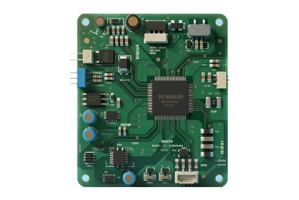
Printed Circuit Boards (PCBs) are fundamental components in the electronics industry. Their primary functions include signal transmission, physical support, power distribution, and thermal management. A PCB comprises various specialized elements: the silkscreen layer (Overlay) for component identification, surface finishes (such as ENIG, HASL), vias for interlayer electrical connections, Through-Hole Components (PTH) and Surface Mount Devices (SMD), copper pours (Polygon), thermal relief pads, signal traces (Track), and pads, among other critical features.
2. PCB Classification System
2.1 Classification by Substrate Material
Ceramic Substrates: Utilizing materials like Alumina (Al₂O₃), Aluminum Nitride (AlN), or Silicon Carbide (SiC), these offer exceptional thermal conductivity and are designed for high-temperature environments and high-power applications.
Metal Core PCBs (MCPCBs): Including Aluminum-based and Copper-based substrates, known for superior heat dissipation, widely used in high-power circuits and LED lighting.
Paper-Based Substrates: Such as FR-1 and FR-2 grades, use fiber paper as reinforcement, impregnated with resin and laminated with copper foil, primarily suitable for single or double-sided boards.
Composite Substrates: Innovatively combine characteristics of multiple materials, e.g., CEM-2 (epoxy resin with a paper core and glass cloth surfaces), to meet specific performance requirements.
2.2 Classification by Structural Characteristics
Rigid PCBs: Use non-bendable rigid substrates, including various types like FR-4 (Glass Epoxy), paper-based, composite, ceramic, and metal core boards.
Flexible PCBs (Flex PCBs): Employ flexible insulating substrates, allowing bending, rolling, and folding, ideal for the space constraints of portable electronic devices.
Rigid-Flex PCBs: Intelligently integrate rigid zones and flexible zones, offering both structural strength and installation flexibility.
HDI PCBs (High-Density Interconnect): Utilize microvia technology and ultra-thin copper foils to meet the miniaturization demands of electronic devices. Structures include 2-step stacked vias, 2-step staggered vias, and 1-step HDI.
IC Substrates: Designed specifically for chip packaging, providing critical functions like electrical connection, physical protection, structural support, and thermal management.
3. In-Depth Analysis of PCB Substrate Technology
3.1 Layer Stack-up Structure
Modern PCBs feature a multi-layer design:
- Core: Laminate composed of glass fiber cloth and epoxy resin, clad with copper on both sides.
- Prepreg (Pre-impregnated): A composite of glass fiber cloth and partially cured resin, responsible for bonding layers together during lamination.
- Copper Foil: Divided into Electro-Deposited (ED) copper (preferred for rigid boards) and Rolled Annealed (RA) copper (used for flexible boards). Thickness is measured in ounces (OZ), e.g., 1 OZ (≈35µm).
3.2 Via Technologies
PCB interconnect vias are categorized into three types:
- Through-Hole Via: Passes through all circuit layers.
- Blind Via: Connects an outer layer to one or more inner layers, but does not go through the entire board.
- Buried Via: Located entirely within the inner layers, connecting two or more internal layers without reaching the outer surfaces.
3.3 Key Performance Parameters
Thermal Parameters:
- Tg (Glass Transition Temperature): The critical point where the resin transitions from a rigid to a softer state, directly impacting the substrate’s heat resistance.
- Td (Decomposition Temperature): The temperature at which the resin loses 5% of its mass due to thermal degradation.
- CTE (Coefficient of Thermal Expansion): Determines dimensional stability under temperature variations. Typically X/Y: 16-18 ppm/°C, Z: 40-60 ppm/°C.
Electrical Parameters:
- Dk (Dielectric Constant): Influences signal propagation speed and characteristic impedance. A lower Dk generally allows faster signal speed (V = C/√Dk).
- Df (Dissipation Factor): Affects signal integrity and quality; lower Df means less signal loss.
- Surface/Volume Resistivity: Measures conductive performance.
Mechanical Parameters:
- Flexural Strength & Peel Strength
- Water Absorption: Impacts substrate stability and reliability. Moisture can increase Dk and risk delamination (“popcorning”).
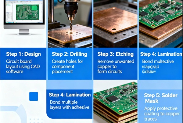
4. Precision PCB Manufacturing Process Flow
PCB fabrication follows a stringent sequence:
- Inner Layer Imaging → 2. Photoresist Lamination → 3. Exposure → 4. Development → 5. Etching → 6. Strip Resist → 7. Layer Stack-up → 8. Lamination → 9. Drilling → 10. Plating (PTH) → 11. Outer Layer Resist Lamination → 12. Exposure → 13. Development → 14. Pattern Plating (Cu/Sn) → 15. Strip Resist → 16. Etching → 17. Tin Strip → 18. Silkscreen/Legend Printing → 19. Surface Finish
5. Comprehensive Comparison of Surface Finish Treatments
| Surface Finish | Key Characteristics & Advantages | Limitations / Challenges | Cost Level | Thickness Range (µm) | Shelf Life |
|---|---|---|---|---|---|
| HASL (Lead-Free) | Suitable for large pads, wide spacing | Not ideal for HDI; high temp; uneven surface | Medium-High | 2-5 (on pad) | 12 months |
| HASL (Lead-Based) | Excellent mechanical strength | Environmental concern (Pb content) | Medium-High | 2-5 (on pad) | 12 months |
| OSP | Simple process, low cost | Not suitable for multiple reflows; difficult inspection | Lowest | 0.1 – 0.5 | 6 months |
| ENIG (Electroless Ni/Immersion Au) | Reliable soldering, flat surface, good corrosion resistance | Potential for “Black Pad” (Ni corrosion), “Gold Embrittlement” | High | Ni: 3-5 / Au: 0.03-0.08 | 12 months |
| ENEPIG (Electroless Ni/Pd/Immersion Au) | High-end apps, superior corrosion resistance, wire bondable | Complex process control, potential for black pad/discoloration | High | Ni:2-5 / Pd:0.05-0.15 / Au:0.05-0.15 | 6 months |
| Immersion Silver (ImAg) | Flat surface, suitable for multiple reflows | Tarnishes easily, requires strict storage conditions | Medium | 0.1 – 0.5 | 12 months |
| Immersion Tin (ImSn) | Good flatness, solderability | Tin whisker risk, poor heat aging resistance | Low | 0.8 – 1.2 | 6 months |
| Electrolytic Ni/Au (Soft Gold) | Excellent wear resistance, contact reliability | High gold consumption, potential solder mask adhesion issues on gold | Highest | Ni: 3-5 / Au: ≥0.05 (selective) | 12 months |
| Electrolytic Hard Gold | Extreme wear resistance (e.g., for fingers) | Highest cost, most complex process | Highest | 0.3 – 3.0 (on contact) | 12 months |