Electronic equipment in the working process will inevitably generate heat, resulting in a rapid rise in internal temperature. If this heat can not be effectively emitted promptly, the equipment will continue to warm up, which in turn triggers overheating failure of components, and ultimately seriously affects the reliability and service life of the equipment.
Therefore, good thermal design for PCB circuit boards is critical, as it is directly related to the stable operation of electronic equipment and long-term reliability. So, in practice, how should we optimize the thermal performance of the PCB?
Table of Contents
1. Analysis of key factors affecting PCB thermal performance
PCB design-related factors
(1) Copper layer design optimization
- Copper paving area: positively correlated with the cooling effect, expanding the copper paving can reduce the junction temperature by 15-25%.
- Copper thickness selection: 2oz and above copper thickness is recommended to enhance thermal conductivity.
(2) Through-hole thermal management design - Thermal perforation array: can reduce junction temperature by 8-12℃ and improve temperature uniformity in the thickness direction.
- Through-hole parameter optimization:
✓ Suggested hole diameter: 0.2-0.3mm
✓ Pitch recommendation: 1-1.5mm
✓ Arrangement: the use of a matrix-type uniform distribution
(3) Special structure design - Dogbone heat dissipation structure: increase the effective heat dissipation area by 30-40%.
- Soldermask design: top/bottom layer fully soldermasked can increase the heat dissipation efficiency by 5-8%.
Substrate material and structure factors
(1) Influence of laminated structure
- 4-layer boards can improve thermal performance by 35-45% compared to double-sided boards.
- A symmetrical laminated structure is recommended
(2) Substrate material selection - A high thermal conductivity substrate (e.g. metal substrate) can improve thermal efficiency by 60-80%.
- Ceramic substrates are suitable for ultra-high power density scenarios.
Environmental and System Level Factors
(1) Airflow optimization design
- Layout principles:
✓ High-power devices downstream of the airflow
✓ Sensitive devices upstream of the airflow - Channel design: maintain a minimum flow resistance path
(2) Aerodynamic optimization - The impact of wind speed: every increase in wind speed of 1m / s, the thermal efficiency of about 15-20% increase
- Turbulence design: A Reasonable setup of the turbulence structure can enhance the heat transfer effect.
(3) System integration considerations - Component spacing: Maintain a minimum spacing of 3-5mm to ensure smooth airflow.
- Structural coordination: Ensure good coupling with the chassis cooling system.
Note: The actual design needs to be combined with thermal simulation tools for multi-parameter optimization; there is a coupling effect between the factors; it is recommended to use orthogonal test methods to determine the best combination of parameters. For application scenarios with a power density of more than 10W/cm², it is recommended to use active cooling solutions to assist.
2. Thermal management solutions for PCB substrate materials
Thermal limitations of traditional PCB materials
PCB substrate materials currently used in mainstream applications include:
- Copper-clad / epoxy glass cloth substrate
- Phenolic resin glass cloth substrate
- Paper-based copper-clad laminates (a small number of applications)
Although these materials have excellent electrical properties and processing characteristics, their thermal conductivity is significantly deficient: - Resin substrates have low thermal conductivity and cannot effectively conduct heat
- Relies heavily on natural convection from the component surface to the surrounding air to dissipate heat
Modern electronic design brings thermal challenges
With the development of electronic equipment to miniaturization, the high-density integration direction, the heat dissipation problem is increasingly prominent:
- Component size continues to shrink, the effective heat dissipation area is greatly reduced
- QFP, BGA, and other surface mount components are widely used, so that the PCB has become the main path of heat conduction
- Power density continues to increase, the traditional heat dissipation methods can not meet the demand
Thermal Optimization Solutions
In response to the above challenges, the most effective thermal management strategy is:
- Enhance the thermal conductivity of the PCB substrate itself.
- Optimize the heat conduction path from the heat-generating components to the PCB.
- Optimize the heat transfer path from the heat-generating components to the PCB. Improve the efficiency of heat dissipation from the PCB to the environment
Key realization paths include:
(1) Adopting high thermal conductivity substrate materials.
(2) Optimize the layout of copper foils and the design of heat-conducting holes.
(3) Combining thermal interface materials to improve heat transfer efficiency.
3. PCB Component Layout Scheme
Component Arrangement Direction
For devices that use natural convection heat dissipation, it is recommended that integrated circuits and other components be arranged in vertical or horizontal order to form the best airflow channels.
Thermal partition layout principles
(1) Partition according to heat generation characteristics:
- Low-power or heat-sensitive components (such as small-signal transistors, small-scale ICs, electrolytic capacitors, etc.) are arranged in the upstream of the cooling airflow (near the air inlet)
- High-power or heat-resistant components (such as power tubes, large-scale ICs, etc.) should be placed downstream of the airflow.
Space layout strategy
(1) Horizontal direction:
- High-power devices should be arranged close to the edge of the PCB to shorten the heat conduction path
(2) Vertical direction: - High-power devices are recommended to be placed in the upper area of the PCB to reduce the thermal impact on other components.
Airflow channel design
(1) to avoid the formation of airflow dead zones on the PCB to ensure smooth air circulation
(2) Multi-board system needs to be considered in the overall airflow distribution
(3) Pay attention to the characteristics of the airflow, naturally choose a low-resistance path, and a reasonable configuration of the component density
Protection of heat-sensitive components
(1) Temperature-sensitive devices should be placed in low-temperature areas (such as the bottom of the equipment)
(2) Strictly prohibit the arrangement of sensitive devices in the heat element directly above the
(3) It is recommended to use a horizontal staggered layout
High-power components to deal with
(1) The main heat source will be arranged in the best location for heat dissipation
(2) Avoid placing high-heat devices in the corners of the board (without auxiliary heat dissipation)
(3) Power resistors should be packaged in larger packages with sufficient space for heat dissipation.
Thermal balance design
(1) Avoid localized thermal aggregation
(2) Try to evenly distribute power devices
(3) to maintain the PCB surface temperature field uniformity
Wiring thermal optimization
(1) Make full use of the thermal conductivity of copper foil
(2) Improve the coverage of copper foil in the wiring layer
(3) Reasonably set up the thermal conductivity of the array of holes
4. Efficient Heat Dissipation Solution
Localized heat dissipation solution (applicable to less than 3 heat-generating devices)
(1) Basic heat dissipation configuration:
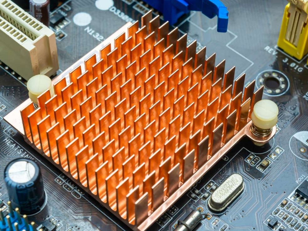
- Installation of separate heat sinks for high heat-generating devices
- Use of heat pipes to enhance the efficiency of heat conduction
(2) Enhanced heat dissipation program: - When passive heat dissipation is insufficient
- Add an active fan cooler combination
- Enhance the heat dissipation efficiency by 30-50%.
Overall heat dissipation program (applicable to more than three heat-generating devices)
(1) Customized thermal solution:
- Customize the overall heat sink according to the device layout
- Precise matching of component height and position
- CNC machining to ensure contact accuracy
(2) Performance optimization measures: - Installation of flexible thermally conductive phase change material spacers
- Compensate for component welding height tolerance
- Improve the thermal conductivity of the contact surface by 60%.
(3) Caution: - Consider the overall structural strength
- Reserve appropriate space for thermal expansion
- Pay attention to the airflow channel design
Mixed heat dissipation strategy
- Combine the advantages of local and overall heat dissipation
- Dual heat dissipation for critical heat-generating components
- Optimize system-level thermal performance
Note: In practice, it is necessary to choose the right combination of thermal solutions according to the specific thermal load, space constraints, and cost budget.