PCB assembly as the core of electronic product manufacturing, the level of its process directly determines the performance and quality of electronic products. Today we explore together, from the basic process to cutting-edge technology, for you to fully analyze the mystery of this precision process.
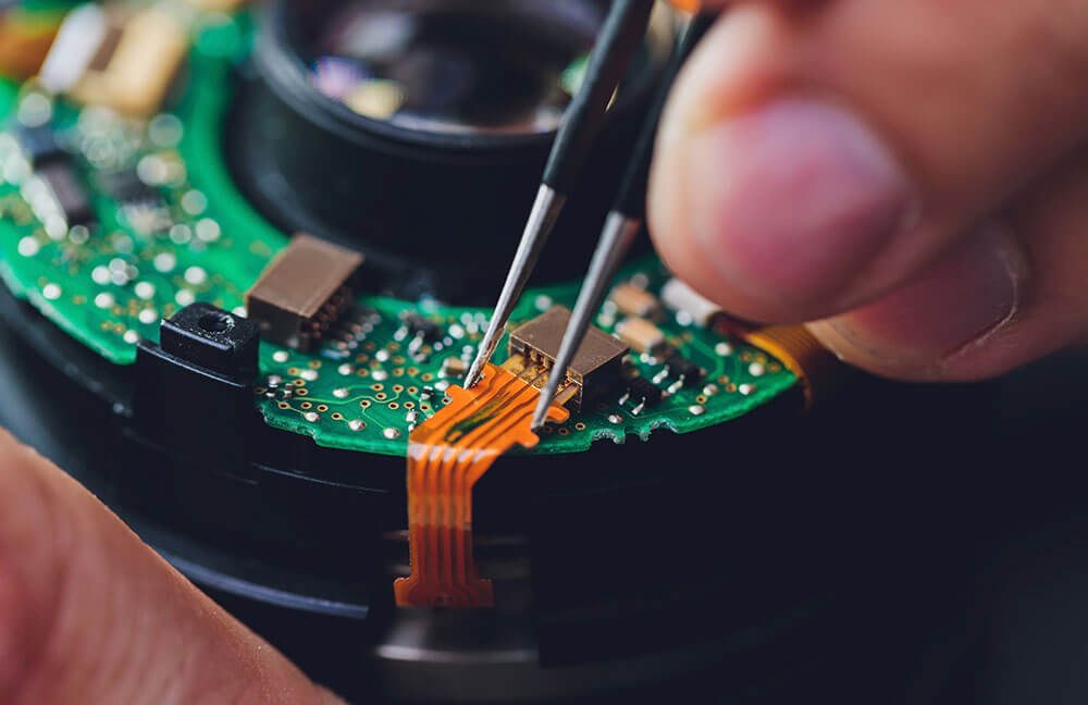
Table of Contents
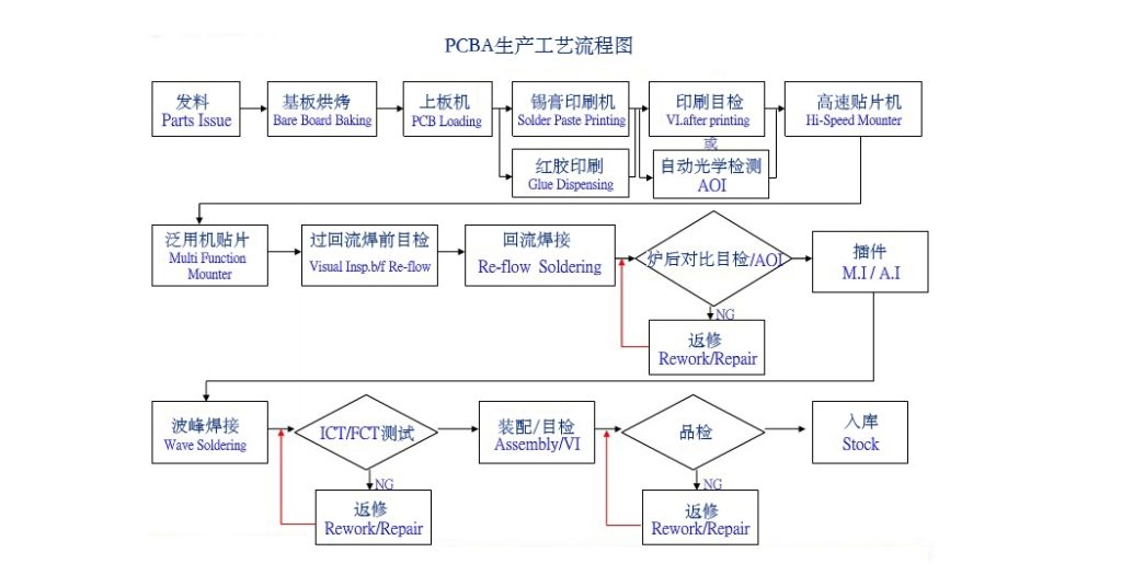
I. Basic PCB assembly process
Solder Paste Printing: A Precise Starting Point
Solder paste printing is the first step in PCB assembly, and its accuracy directly affects the subsequent welding quality. Currently the mainstream use of stencil printing technology, through laser cutting or electroforming to produce high-precision stencil, the solder paste is uniformly printed to the PCB pads. The control of the amount of solder paste is extremely important, too much may lead to bridging, and too little may lead to false soldering, so it needs to be precise and accurate.
Component placement: the art of high precision
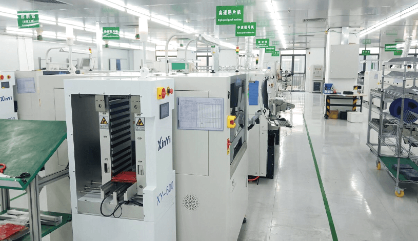
Component placement is the process of accurately placing electronic components into the corresponding position on the PCB, and the SMT placement machine can complete the rapid placement of components with micron-level precision through the high-precision visual recognition system and robotic arm. Whether it’s a tiny resistor or capacitor, or a complex integrated circuit, SMT machines can complete the process efficiently, so first-class production equipment is indispensable.
Reflow Soldering: Solid Connections
Reflow soldering is the process of firmly soldering components to a PCB by heating it so that the solder paste melts. Reflow ovens use a precise temperature control system, which is needed to ensure that the soldering temperature profile meets the requirements and to avoid soldering defects, such as false soldering, bridging, or component damage, caused by too high or too low temperatures.
Inspection and Rework: The Guardian of Quality
After the soldering is completed, automatic optical inspection (AOI) equipment quickly detects solder joint defects through high-resolution cameras and image recognition algorithms. The detected defective solder joints are usually reworked by manual welding or laser welding to ensure that each solder joint meets the quality standard before normal delivery to customers.
Cleaning and Testing: The Final Guarantee
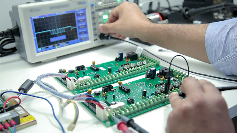
Solder paste residues and fluxes are generated during the soldering and rework process and need to be removed through the cleaning process to avoid affecting circuit performance. After cleaning, the PCB also needs to be functionally tested to ensure that its electrical performance and functionality meets the design requirements, ensuring that this board can work properly.
Second, PCB assembly cutting-edge technology
High-Density Interconnect (HDI): smaller, denser, and stronger
With the development of electronic products to miniaturization, and high performance, PCB wiring density needs to be constantly improved, HDI technology using microvias, blind holes, buried holes, and other advanced processes, to achieve a finer line layout, to meet the needs of high-density interconnection. This technology is widely used in smartphones, wearable devices, and other high-end electronic products.
Advanced Packaging Technology: Breakthrough Performance Bottleneck
Traditional packaging technology can no longer meet the needs of high-performance chips, advanced packaging technology such as 3D packaging, system-in-package (SiP), and so on came into being. These technologies integrate multiple chips into a single package, significantly improving system performance and reliability while reducing space requirements.
Automation and Intelligence: A Leap in Efficiency and Quality
The application of automation equipment and artificial intelligence technology is driving PCB assembly in the direction of intelligence. Automated production lines can realize full-process automated production from raw materials to finished products, significantly improving efficiency and reducing human error. Artificial intelligence technology is used for defect detection, process optimization, and other links to further improve production efficiency and product yield. The application of automation equipment and artificial intelligence technology makes PCB assembly more efficient and accurate.
Third, the future development trend of PCB assembly
Green is the inevitable choice for sustainable development
With the enhancement of environmental awareness, the PCB assembly process is moving in the direction of green development. Lead-free solder, water-based cleaning agents, and other environmentally friendly material applications are reducing pollution emissions in the production process, reducing the impact on the environment, and promoting the sustainable development of the electronics manufacturing industry.
Flexible electronics: adapting to the future shape
Flexible electronics is an important direction for the future development of the electronics industry, PCB assembly technology also needs to adapt to the characteristics of flexible substrates and the development of new processes and equipment. Flexible PCB assembly technology has a broad application prospect in the field of wearable devices, folding screen cell phones, and other fields.
Heterogeneous integration: the future of multifunctional integration
Heterogeneous integration technology integrates components of different materials and processes to realize more complex functions.PCB assembly technology needs to be combined with heterogeneous integration technology to develop new interconnect and packaging solutions to meet the high-performance needs of future electronic systems.
Conclusion: PCB assembly – the precision art of electronic manufacturing
PCB assembly process is a key technology in the field of electronics manufacturing, its level of development directly affects the progress of the electronics industry, PCB assembly will be more intelligent, efficient, and environmentally friendly. From the basic process to cutting-edge technology, PCB assembly has always been in constant innovation and breakthroughs, for the performance of electronic products and functional expansion to provide strong support. PCB assembly is like the electronic products of the “building blocks” art, it is a variety of components skillfully combined to give life to electronic products. In the future, with the further development of green, flexible electronics and heterogeneous integration technology, PCB assembly will continue to lead the electronics manufacturing industry to new heights, laying a solid foundation for the construction of the intelligent world.