Table of Contents
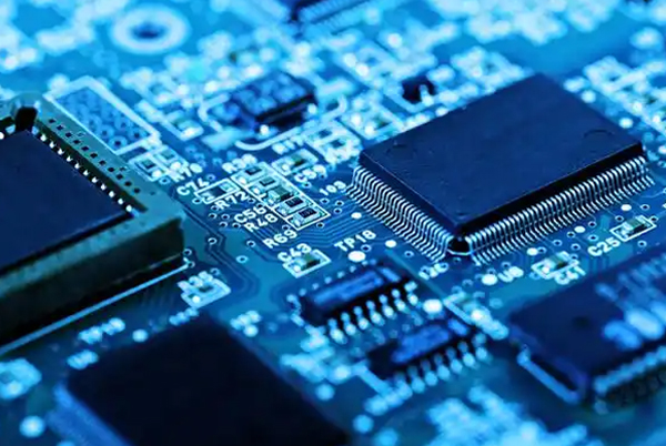
Microvia Technology in High-Density Printed Circuit Boards
As electronic devices shrink and performance requirements increase, 14-layer printed circuit board designs are becoming a necessity for advanced applications. Microvia technology is at the center of this evolution, enabling unprecedented circuit density and signal integrity.
Why Microvias Are Critical for 14-Layer PCB Performance
Space Optimization Advantages
- 50% higher connection density than conventional through-holes
- Enables 40% more components in the same footprint (critical for server/5G applications)
- Supports HDI (High Density Interconnect) architectures
Signal Integrity Benefits
| Feature | Improvement | Impact |
|---|---|---|
| Path length | 60-70% shorter | Reduces latency |
| Crosstalk | 15-20dB lower | Cleaner signals |
| Impedance control | ±5% tolerance | Better matching |
| Parasitic effects | 40-60% reduction | Sharper edges |
Manufacturing Breakthroughs Enabling Reliable Microvias
Precision Laser Drilling
- UV lasers (355nm) for 50-100μm microvias
- ±10μm positioning accuracy
- Multi-step drilling process for 14-layer stacks
Advanced Plating Techniques
- Direct plating technology
- Pulse electroplating for uniform coverage
- ±3μm thickness control
Layer Alignment Solutions
- X-ray alignment systems (±25μm)
- CTE-matched materials prevent warping
- Optical fiducials for registration
Three Common Problems and Solutions in 14-Layer PCB Microvia Design
Problem 1: Incomplete Microvia Plating Leading to Unreliable Connections
Q: During testing of 14-layer PCB prototypes, some inner-layer microvias show incomplete plating, causing intermittent interlayer connections. How can this be resolved?
A: This issue is typically caused by three factors:
- Insufficient post-drilling cleaning, leaving resin residues that hinder copper adhesion. Solution: Optimize desmear processes using combined plasma and chemical cleaning.
- Poor electrolyte flow, trapping air bubbles in deep vias. Solution: Switch to oscillating plating tanks to improve solution flow and adjust parameters with reverse-pulse current.
- Moisture absorption in substrates degrades drilling quality. Solution: Pre-bake boards at 120°C for ≥4 hours before drilling.
Problem 2: Severe Signal Reflections at Microvias in High-Speed Traces
Q: In a 10 Gbps high-speed signal path, eye diagrams show significant reflections and jitter when transitioning through microvias. How can this be optimized?
A: Signal reflections at microvias stem from impedance discontinuities. Solutions include:
- Back-drilling (stub removal): Remove unused via portions to eliminate excess copper stubs. For 14-layer boards, back-drilling depth control should be within ±50 μm.
- Optimize reference planes: Ensure each signal microvia has a complete ground return path, ideally with at least three grounding microvias for shielding.
- Add compensation capacitors: Use simulation to determine optimal capacitance (typically 0.5–2 pF) to counteract parasitic inductance.
Problem 3: Thermal Stress-Induced Microvia Cracking
Q: After thermal cycling tests, some microvias—especially near board edges—develop cracks or fractures. How can this be mitigated?
A: This is a classic thermomechanical reliability issue. Solutions include:
- Material selection: Use high-Tg (>170°C) substrates with matched CTE, such as Panasonic’s MEGTRON 6 or Isola’s FR408HR, which offer Z-axis CTE below 50 ppm/°C.
- Design optimization: Avoid dense microvia arrays within 3 mm of board edges; use teardrop-shaped pads for critical microvias to enhance mechanical strength.
- Process control: Optimize lamination profiles with stepwise heating/pressure to minimize residual stress, and add stress-relief annealing post-curing.
Best Practices for 14-Layer PCB Microvia Design
Microvia technology has become indispensable for high-performance electronic systems in 14-layer PCB design. Key takeaways from this analysis include:
- High-density interconnects and optimized signal routing enable 14-layer PCBs to integrate complex functionalities in compact spaces while enhancing signal integrity.
- Successful microvia design requires balancing electrical performance, thermomechanical reliability, and manufacturability.
- Proven solutions exist for common issues—early risk identification and DFM (Design for Manufacturing) principles are crucial for prevention.
- Emerging technologies like laser direct imaging and 3D-printed microvias promise to push the boundaries of current design capabilities, particularly for 5G, AI, and HPC applications.
For design teams, mastering microvia principles and troubleshooting methods will significantly improve first-pass success rates, accelerate development cycles, and secure a competitive edge in fast-evolving markets.
Latest Featured Articles
- Turnkey PCBA Supplier: How to Source Complete Assembly Services
- Why Choose a Reliable PCBA Supplier for Your Electronics Projects
- Which PCB Company Specializes in PCB Assembly? A Deep Dive into High-Precision Manufacturing
- Let’s Connect in Moscow: Topfast Invites You to ExpoElectronica 2026
- Power Electronics PCB Design for EV