PCB (Printed Circuit Board) is the core component of modern electronic devices. Understanding its manufacturing process is crucial for both electronics enthusiasts and professionals. This article adopts a Q&A format to detail the complete PCB fabrication process, covering every step from design to finished product while maintaining both professionalism and accessibility.
Table of Contents
Basic Concepts of PCB Manufacturing
What is a PCB, and why is it so important?
A PCB (Printed Circuit Board) is a substrate used to support and connect electronic components, achieving electrical connections between components through copper traces. It serves as the backbone of all electronic devices, from smartphones to spacecraft.
The importance of PCBs manifests in three aspects:
- Reliability: Replaces hand-soldered flying wires, reducing connection errors
- Standardization: Enables mass production and automation of electronic devices
- High Density: Modern multilayer PCBs can implement complex circuits in limited space
What are the main methods for making PCBs?
Depending on the production environment and requirements, there are several primary PCB fabrication methods:
- Professional Factory Production:
- Suitable for: Mass production, high-precision requirements
- Processes: Photochemical methods, electroplating processes
- Layers: Can produce single-sided, double-sided, and multilayer boards (4-layer, 6-layer or more)
- DIY Handmade Methods:
- Suitable for: Prototyping, simple circuits
- Common methods:
Heat Transfer Method: Uses a heat press machine to transfer printed circuit patterns from special paper to copper-clad boards
Photosensitive Board Method: Uses photosensitive copper-clad boards with exposure and development processes
Hand Drawing Method: Uses special oil-based pens to draw circuits directly on copper-clad boards
PCB Design Phase
How to begin designing a PCB?
PCB design is the first and most critical step in the manufacturing process:
- Circuit Design:
- Use EDA software (like Altium Designer, Eagle, KiCad) to draw schematics
- Determine component parameters and connection relationships
- PCB Layout:
- Convert schematics to actual PCB layouts
- Consider component placement, trace routing, and interlayer connections
- Design Verification:
- Electrical Rule Check (ERC)
- Design Rule Check (DRC)
- Signal Integrity Analysis (for high-frequency circuits)
What professional PCB design software is recommended?
Depending on needs and skill level, consider these options:
| Software | Target Users | Features | Price |
|---|---|---|---|
| Altium Designer | Professional Engineers | Comprehensive features, industry standard | High |
| Eagle | Small-Medium Businesses | Rich component libraries, Autodesk product | Medium |
| KiCad | Hobbyists/Students | Open source, powerful features | Free |
| Proteus | Education Sector | Combining simulation with PCB design | Medium |
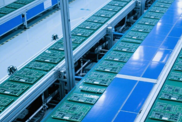
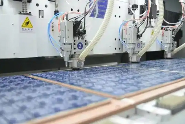
Professional PCB Factory Manufacturing Process
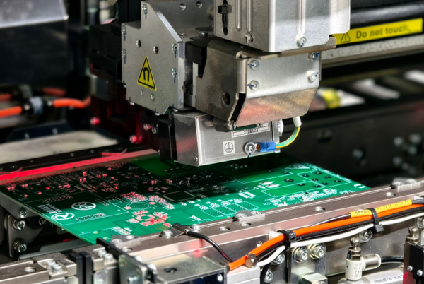
What does the professional PCB factory manufacturing process look like?
Professional PCB factory processes are complex and precise. Taking a 4-layer board as an example:
- Inner Layer Production:
- Core board cleaning → Photoresist coating → Exposure → Development → Etching → Stripping
- Lamination:
- Stack core boards with prepreg (pre-impregnated materials)
- High temperature and pressure bonding
- Drilling:
- Mechanical drilling or laser drilling
- Creates through-holes, blind vias or buried vias
- Hole Metallization:
- Electroless copper deposition → Electroplating thickening
- Makes the walls conductive for interlayer connections
- Outer Layer Production:
- Similar photolithography process as inner layers
- Pattern plating to increase copper thickness
- Solder Mask & Silkscreen:
- Apply solder resist ink (typically green)
- Print component identifiers and reference designators
- Surface Finish:
- Options like HASL, ENIG, OSP
- Protects pads and improves solderability
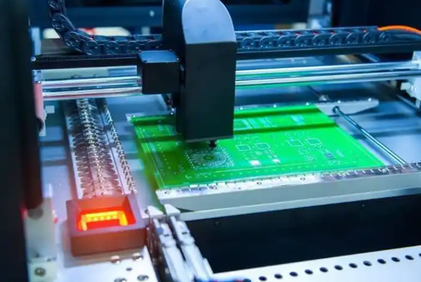
- Routing & Testing:
- Milling or V-cut scoring
- Electrical testing (flying probe or test fixture)
Why do multilayer PCBs require such complex processes?
The complexity of multilayer PCBs (like 4-layer or 6-layer boards) stems from:
- Layer Alignment: Each layer’s circuits must align precisely (typically <50μm tolerance)
- Interlayer Insulation: Must maintain insulation between signal layers
- Reliable Interconnects: Plated through-holes ensure layer connections with conductive continuity
- Signal Integrity: High-frequency signals require impedance control and crosstalk consideration
These requirements make multilayer PCB manufacturing a precision process combining electronics, chemical engineering, and mechanical technologies.
DIY PCB Fabrication Methods
How to make simple PCBs at home?
For electronics hobbyists, the heat transfer method is commonly used:
Materials Needed:
- Copper-clad board (single or double-sided)
- Laser printer
- Heat transfer paper
- Etching solution (ferric chloride or hydrochloric acid + hydrogen peroxide)
- Drilling tools (small electric drill)
Steps:
- Design & Print:
- Complete layout using PCB design software
- Print the mirror image on heat transfer paper
- Pattern Transfer:
- Press the printed side onto the cleaned copper-clad board
- Apply heat using an iron or a heat press machine (160-200°C)
- Etching:
- Submerge in the etching solution to remove exposed copper
- Monitor the process to avoid over-etching
- Cleaning & Drilling:
- Remove the transfer toner with solvent
- Drill holes according to component lead sizes
- Solder Preparation:
- Apply rosin flux solution to prevent oxidation
- Verify circuit connectivity
What precautions should be taken for DIY PCB fabrication?
- Safety First:
- Etching solutions are corrosive—wear gloves and goggles
- Work in well-ventilated areas
- Precision Control:
- Recommended minimum trace width: 0.3mm
- Recommended minimum clearance: 0.2mm
- Troubleshooting:
- Incomplete transfer: Touch up with an oil-based pen
- Incomplete etching: Check solution concentration and temperature
- Drilling misalignment: Use a center punch first
- Environmental Considerations:
- Collect and properly dispose of waste etching solution
- Never pour down drains
Advanced PCB Knowledge
How to choose appropriate PCB materials?
PCB material selection considers these factors:
- Base Material Types:
- FR-4: Most common, fiberglass epoxy, cost-effective
- High-Frequency Materials: Like Rogers, for RF/microwave circuits
- Flexible Materials: Polyimide, for flex circuits
- Key Parameters:
- Tg (Glass Transition Temperature): ~130-140°C for standard FR-4
- Dielectric Constant: Affects signal propagation speed
- Loss Tangent: Critical for high-frequency applications
- Copper Weight Selection:
- Standard: 1oz (35μm)
- High Current: 2oz or thicker
- Precision Signals: 0.5oz allows finer traces
What are the PCB surface finish options and their characteristics?
Comparison of common PCB surface finishes:
| Finish Type | Advantages | Disadvantages | Typical Applications |
|---|---|---|---|
| HASL | Low cost, good solderability | Uneven surface, not for fine pitch | Consumer electronics |
| ENIG | Flat surface, oxidation resistant | Higher cost, black pad risk | HDI boards, contact points |
| OSP | Low cost, simple process | Short shelf life, limited rework | Short-life consumer products |
| Immersion Silver | Good solderability, high-frequency suitable | Prone to oxidation, special packaging needed | RF circuits, automotive |
| Electrolytic Gold | Low contact resistance, wear-resistant | Highest cost | Connectors, high-reliability |
PCB Quality Control and Testing
How to ensure PCB manufacturing quality?
PCB quality control spans the entire production process:
- Raw Material Inspection:
- Copper-clad board thickness and quality
- Prepreg resin content and flow characteristics
- Process Control:
- Trace width/space measurement (typically optical equipment)
- Hole wall quality inspection (cross-section analysis)
- Layer-to-layer alignment verification
- Final Testing:
- Electrical testing (opens/shorts)
- Impedance testing (for high-speed designs)
- Solderability testing
- Reliability Testing (as needed):
- Thermal stress testing (e.g., 288°C solder float)
- Humidity aging tests
- Mechanical strength tests
What are common PCB defects and how can we prevent them?
Common defects and preventive measures:
- Opens/Shorts:
- Cause: Incomplete etching or over-etching
- Prevention: Optimize etch parameters, increase inspection frequency
- Hole Wall Separation:
- Cause: Poor drilling quality or electroless copper issues
- Prevention: Improve drilling parameters, enhance hole cleaning
- Pad Lifting:
- Cause: Excessive thermal stress or poor adhesion
- Prevention: Optimize soldering profile, select high-Tg materials
- Impedance Deviation:
- Cause: Inconsistent dielectric thickness or trace width
- Prevention: Tight dimensional control, precision processing equipment
PCB Manufacturing FAQ
How long does PCB manufacturing take?
Production time depends on process complexity and factory schedule:
- Standard Processes:
- Single-sided: 1-2 days
- Double-sided: 2-3 days
- 4-layer: 3-5 days
- Special Processes:
- Impedance-controlled: Add 1-2 days
- Heavy copper (≥3oz): Add 2-3 days
- Blind/buried vias: Add 3-5 days
Note: Above are production times, excluding logistics. Rush services typically reduce time by 30-50% at a higher cost.
What factors determine PCB manufacturing costs?
Primary cost factors:
- Material Costs (~20-30% of total):
- Base material type (FR-4 vs high-frequency)
- Board thickness and copper weight
- Special materials (e.g., metal core)
- Process Costs (~40-50% of total):
- Layer count (each additional layer increases cost 30-50%)
- Hole size and quantity (small holes <0.3mm increase cost)
- Surface finish type
- Design Complexity Costs:
- Trace width/space (finer features increase cost)
- Special requirements (impedance control, blind vias)
- Order Quantity:
- Small batches (<5m²) have higher unit cost
- Large volumes significantly reduce per-unit cost
Future Trends in PCB Technology
What are emerging directions in PCB technology?
PCB technology continues evolving with key trends including:
- High Density Interconnect (HDI):
- Finer traces/spaces (down to 50μm/50μm)
- More microvias (laser drilling technology)
- Flexible/Rigid-Flex Boards:
- Adaptable for wearables and foldable devices
- Enables 3D assembly, saves space
- Embedded Components:
- Bury passive components within the PCB
- Increases integration, improves electrical performance
- Green Manufacturing:
- Lead-free, halogen-free materials
- New processes reducing chemical waste
- Smart PCBs:
- Integrated sensors and data processing
- Enables self-monitoring and diagnostics
Through this detailed guide, you should now have a comprehensive understanding of the complete PCB fabrication process. Whether choosing professional manufacturing or DIY approaches, grasping these principles and techniques will help you obtain better PCB products. As technology advances, PCB manufacturing processes continue innovating, providing the foundation for electronic device miniaturization and high-performance applications.
More related reading
1.Printed Circuit Board(PCB)
2.Printed Circuit Board (PCB) Types
3.PCB Design and Manufacturing
4.Common Problems and Solutions in PCB Design
5.What do the letters on the PCB mean?
6.PCB Fabrication And Assembly