Table of Contents
What is PCB layout, and its importance?
If you want to ensure the reliability of PCB products, you must first do the following three things
- What is PCB?
- Why PCB layout?
- PCB layout: How to ensure reliability?
1. What is the PCB?
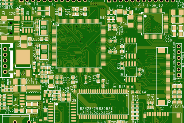
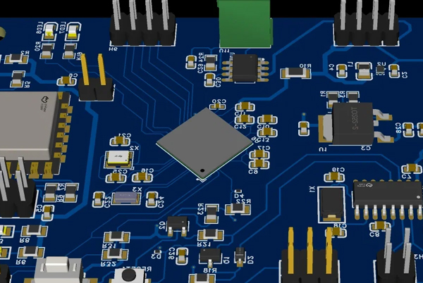
PCB is the core carrier of modern electronic products, which connects various electronic components through precise copper foil alignment to realize the function of circuit design and provide mechanical support.
Electronic Component Symbols and Terminology
Standardized abbreviations for electronic components
- RES: Resistor
- CAP: Capacitor
- IND: Inductor
- LED: Light Emitting Diode
- IC: Integrated Circuit
PCB Electronics Terminology
- Voltage (V): Potential difference, measured in volts
- Current (I): Electron flow, measured in amperes
- Resistance (R): Ability to impede current, measured in ohms
- Ohm’s Law: V = I×R
- Kirchhoff’s Laws: Including Current Law (KCL) and Voltage Law (KVL)
PCB Layer Structure and Material Selection
Common PCB layer structure types:
- Single-sided boards: Lowest cost, suitable for simple circuits
- Double-sided boards: Traces on both sides connected through vias
- Multilayer boards (4-12 layers): Preferred for complex circuits with dedicated power and ground planes
Common substrate materials:
- FR-4: Glass-reinforced epoxy laminate, most commonly used
- High-frequency materials, Such as Rogers RO4003C for RF circuits
- Flexible materials: Polyimide for bendable circuits
2. Why PCB layout?
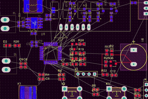
PCB layout refers to the schematic diagram in the actual circuit board design process, including component placement, alignment planning, interlayer connection, and other key steps. An excellent PCB layout not only ensures that the circuit works properly but also significantly improves the product’s electromagnetic compatibility (EMC), thermal performance, and long-term reliability.
According to statistics, about 70% of electronic product failures are from PCB design problems, rather than defects in the components themselves. Therefore, mastering professional PCB layout skills is critical for electronic engineers.
Understand clearly after understanding the above two points clearly, we mainly explore the third point today. To ensure the reliability of the PCB, what should be done?
PCB layout: How to ensure reliability?
Core Principles and Techniques of PCB Layout
Component Placement Standards
- Minimum spacing principle:
- ≥2mm distance between components and board edge (5mm recommended)
- High-voltage component spacing: Add at least 1mm per 1000V
- Functional partitioning:
- Strict separation of digital/analog circuits
- Dedicated areas for high-frequency circuits
- Arrangement following signal flow (input → processing → output)
- Orientation consistency:
- All components should maintain the same orientation (horizontal or vertical)
- Clear polarity markings for polarized components
- Soldering considerations:
- Wave soldering component spacing: 50- 100 mil (1.27-2.54mm)
- Reflow soldering allows slightly smaller spacing
Power and Ground Plane Design Essentials
Power integrity directly affects system stability. Excellent designs should:
- Layer strategy:
- Dedicated power and ground layers in multilayer boards
- Adjacent power/ground planes forming natural capacitance
- Trace specifications:
- Ground trace width > power trace > signal trace
- Critical power traces using “star” or “grid” topologies
- Decoupling capacitor placement:
- 0.1μF capacitor near each power pin
- One 10μF bulk capacitor per 5-10 ICs
- Capacitors are placed as close as possible to the power pins
- Grounding techniques:
- Single-point connection for digital/analog grounds
- Multi-point grounding for high-frequency circuits
- Avoid ground loops
Signal Integrity Management
- Priority routing:
- Route clocks, high-speed differential pairs first
- Maintain equal length, symmetrical routing
- 3W rule:
- Center-to-center spacing ≥3×trace width
- Reduces crosstalk
- Impedance control:
- Calculate characteristic impedance for high-speed signals
- Maintain consistent impedance in differential pairs
- Via optimization:
- Minimize vias in high-speed signals
- Use blind/buried vias when necessary
Practical EMC/EMI Design Techniques
Controlling EMI’s Three Elements
- Noise source suppression:
- Shield clock circuits
- Use π-filters for switching power supplies
- Add small series resistors to fast-switching devices
- Coupling path blocking:
- Keep sensitive signals away from noise sources
- Use guard traces for critical signals
- Increase interlayer distance
- Sensitive circuit protection:
- Separate analog circuits from digital areas
- Local copper pour for high-frequency circuits
- Implement common-mode chokes
Implementation Methods
- Stackup strategy:
- Typical 4-layer stack: Signal-Ground-Power-Signal
- 6-layer boards can add dedicated routing layers
- Filtering techniques:
- Bulk electrolytic capacitors at power inputs
- Ceramic decoupling capacitors at IC power pins
- π-type or T-type filters for signal lines
- Shielding measures:
- Local grounded copper pour in sensitive areas
- Metal shields when necessary
- Ferrite beads at cable ports
Common PCB Layout Problems and Solutions
Problem 1: How to solve signal reflection in high-speed circuits?
Solutions:
- Implement impedance matching: Source-series or end-parallel termination
- Apply appropriate termination strategies: Parallel, Thevenin, etc.
- Control trace length: Keep high-speed traces short and straight
- Avoid sharp angles: Use 45° or curved corners
Problem 2: How to optimize Power Distribution Network (PDN) in multilayer boards?
Solutions:
- Design low-impedance power planes
- Proper decoupling capacitor combinations (large + small values)
- Use power integrity analysis tools for simulation
- Add local power planes near critical ICs
- Maintain tight coupling between power and ground planes
Problem 3: How to effectively reduce digital circuit interference with analog circuits?
Solutions:
- Physical separation: Maintain at least 5mm spacing
- Ground plane partitioning: Single-point connection for digital/analog grounds
- Independent power supply: Use LDOs for analog sections
- Signal isolation: Optocouplers or magnetic couplers for digital-to-analog signals
- Layout optimization: Place analog circuits near board edges to reduce interference paths
Summary
Excellent PCB layout is the cornerstone of electronic product quality. By following the principles and tips below, you can significantly improve your design success:
- Plan first: Complete functional partitioning and stackup design before starting
- Power priority: Dedicate sufficient effort to optimizing power distribution
- Signal focus: Route critical signals first to ensure integrity
- EMC design: Control EMI at the source rather than fixing it afterwards
- Verification testing: Use DRC checks and necessary simulations to validate designs