
In today’s rapidly developing electronics manufacturing industry, printed circuit board quality control has become a critical factor determining product success. As a leading global PCB manufacturer, TOPFAST deeply understands the importance of electrical testing for product quality. We not only provide high-quality PCB products but also offer comprehensive testing solution consultations for our customers.
Table of Contents
Electrical Testing: The Lifeline of PCB Quality
Electrical testing is far more than a simple “pass/fail” judgment—it is the cornerstone ensuring PCB reliability in complex electronic systems. Through precise resistance and insulation resistance measurements, we can detect potential defects invisible to the naked eye, assuring the long-term stability of final products.
In our experience serving global customers, we have found that over 30% of early product failures originate from hidden electrical defects in PCBs. This is precisely why we invest significant resources in optimizing testing processes.
In-depth Analysis of Testing Technologies: Beyond Tool Selection
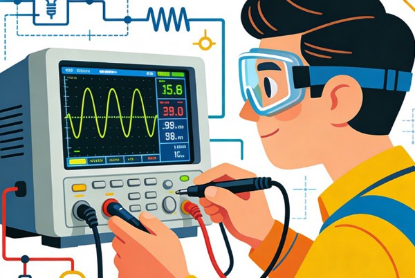
Flying Probe Testing: The Art of Flexibility and Precision
The Logic Behind Technological Evolution:
The development of flying probe testing from simple continuity checks to today’s multifunctional testing platform reflects the electronics manufacturing industry’s urgent need for flexibility and rapid iteration.
- Intelligent Path Optimization Algorithms: Reducing average testing time by 15-20%
- Multilayer Board Testing Strategies: Specialized testing solutions for high-density interconnect boards
- Non-destructive Testing Standards: Ensuring PCB integrity post-testing, meeting the strictest customer requirements
Why Choose TOPFAST’s Flying Probe Testing Services?
We don’t just provide testing equipment—we offer testing strategy optimization based on decades of experience. For R&D stages and small-batch production, our flying probe testing solutions can shorten time-to-market by 40% while reducing testing development costs by 60%.
Adapter Testing: The Efficiency Engine for Mass Production
The Economics of Scale Testing:
When production volume reaches a critical point (typically 500-1000+ pieces), the economic advantages of adapter testing become apparent.
- Rapid Adapter Design Services: Compressing traditional 4-6 week development cycles to 2-3 weeks
- Modular Adapter Systems: Supporting quick adaptation for similar PCB families, reducing repeated investments
- Full Lifecycle Management: Complete adapter services from design to maintenance
Industry Case Study:
Our intelligent adapter testing system, designed for an automotive electronics client, achieved testing capacity exceeding 300 pieces per hour with defect detection rates reaching 99.97%, helping the client reduce field failure rates by 75%.

Technology Integration: The New Era of Intelligent Testing
Hybrid Testing Strategies
Combining the flexibility of flying probe testing with the efficiency of adapter testing, we have developed unique hybrid solutions:
- Use flying probe testing initially to verify design and process
- Employ optimized adapter testing during mass production
- Maintain flying probe sampling capabilities for critical batches
Data-Driven Testing Optimization
Through collecting and analyzing testing data, we can:
- Predict potential process issues
- Optimize the balance between test coverage and time
- Provide design improvement suggestions to enhance quality at the source
AI-Assisted Defect Diagnosis
Our intelligent testing systems can:
- Automatically identify defect patterns
- Provide root cause analysis
- Generate actionable improvement recommendations
Selection Strategy: A Decision Framework Based on Value Maximization
| Decision Dimension | Flying Probe Advantages | Adapter Testing Advantages | TOPFAST Value-Added Services |
|---|---|---|---|
| Time Sensitivity | Quick start (24-48 hours) | Long-term efficiency | Rapid assessment service, providing solution suggestions within 24 hours |
| Cost Structure | No upfront fixture investment | Extremely low per-unit testing cost | Comprehensive TCO analysis to help select optimal solutions |
| Quality Requirements | High precision, adjustable parameters | Stable and consistent testing conditions | Customized testing standard development |
| Product Stage | R&D, prototyping, small batches | Mass production | Smooth phase transition support |
| Technical Complexity | Suitable for high-density, new technologies | Suitable for mature technology mass production | Technical risk assessment and mitigation solutions |
TOPFAST Professional Recommendations:
- For innovative products, adopt a “flying probe first, gradual transition” strategy
- For mature product lines, invest in intelligent adapter systems
- For mixed production environments, utilize our hybrid testing solutions
Future Outlook: Intelligent, Integrated, Sustainable Testing Ecosystem
- Cloud Testing Platform: Remote testing, monitoring, and analysis
- Predictive Maintenance: Equipment health management based on testing data
- Green Testing: Energy consumption-optimized testing strategies
- Full-Process Integration: Seamless data flow from design to testing
Take Action Now: Let TOPFAST Become Your Quality Partner
Regardless of your product development stage, TOPFAST can provide the most suitable testing solutions. We invite you to:
- Schedule a free testing solution consultation: Our expert team will analyze your optimal testing strategy
- Apply for sample testing: Personally experience the precision and efficiency of TOPFAST testing services
- Participate in our testing technology seminars: Deeply understand the latest testing technologies and industry best practices
Contact Us: Visit the TOPFAST official website or call our technical service center. Let’s work together to build a zero-defect electronics world.
In an era where quality determines competitiveness, choosing the right testing strategy means choosing success. Let TOPFAST’s professional knowledge and innovative solutions safeguard your product quality, helping you gain a competitive edge in the intense market competition.
Frequently Asked Questions About Electrical Testing
A: The core difference lies in the balance between flexibility and efficiency. Flying probe testing uses 4-8 movable probes to test points sequentially and does not require dedicated fixtures. It is suitable for the R&D phase, small-batch production, or products requiring rapid iteration. Bed-of-nails testing uses a custom adapter to contact all test points simultaneously, offering extremely high testing efficiency, but it requires investment in fixture costs and time.
TOPFAST Recommendation: If your product is in the R&D verification stage or has a monthly volume of less than 500 pieces, we recommend flying probe testing. If it is a mature product with a monthly output exceeding 1000 pieces, bed-of-nails testing offers better overall cost-effectiveness. We provide a free testing solution evaluation service and can offer customized suggestions based on your product characteristics and production plans.
A: Traditional flying probe testing can indeed leave tiny marks on solder pads, but TOPFAST has solved this issue through technological innovation. Our “soft landing” technology uses precise speed control and pressure management to achieve gentle contact between the probe and the test point. Furthermore, our optimized probe materials and surface treatment technologies further minimize contact marks.
For high-reliability products (such as automotive electronics, medical devices), we have even stricter standards: using specially passivated probes, establishing contact pressure profiles, and employing optical re-inspection to ensure pad integrity. In our aerospace-grade PCB projects, this optimized solution has been validated through 1 million tests, achieving zero damage.
A: Test coverage needs to be determined comprehensively based on the product’s risk level and application scenario. TOPFAST has established a three-tier assessment system:
Basic Coverage (above 95%): Covers all power/ground networks and critical signal paths.
Enhanced Coverage (above 98%): Adds testing for adjacent networks with spacing less than 0.2mm.
Complete Coverage (above 99.5%): Includes all networks and component parameter testing.
Our suggestion: Consumer electronics can opt for 95-98% coverage; industrial control products are recommended to have 98-99%; automotive and medical electronics must achieve above 99.5%. TOPFAST provides coverage analysis and optimization services. We can increase coverage by 15-20% without adding test time through intelligent test sequencing.
A: The designed service life of a standard bed-of-nails adapter under normal operating conditions is 500,000 test cycles. TOPFAST extends service life through three major measures:
Material Optimization: Using military-grade probes and enhanced baseplate materials.
Smart Maintenance: Built-in contact resistance monitoring system to warn of probe wear.
Modular Design: Supports quick replacement of wear-prone components.
A typical maintenance cycle involves a deep service every 100,000 test cycles, costing approximately 5-8% of the adapter’s original price. We recommend the TOPFAST Full Lifecycle Service Package, which includes regular calibration, preventive maintenance, and priority repair. This can extend the adapter’s service life to over 800,000 cycles and reduce overall maintenance costs by 30%.
A: Mixed-signal PCBs require special testing strategies. TOPFAST’s hybrid testing solution includes:
Technical Approach:
Zoned Testing Strategy: Parallel testing for digital circuits, isolated testing for analog circuits.
Dynamic Shielding Technology: Real-time isolation of interfering circuit modules during testing.
Sequencing Optimization Algorithm: Reasonably schedules test orders to avoid signal crosstalk.
Equipment Configuration:
High-Speed Digital Test Channels (up to 1GHz)
High-Precision Analog Measurement Unit (24-bit ADC)
Professional Grounding and Shielding System
Success Case: The hybrid testing solution we designed for a medical imaging equipment client consolidated two originally required independent test stations into one, reducing test time by 40% and lowering the missed detection rate for signal integrity issues from 3.2% to below 0.5%.