Table of Contents
What is a High Speed Printed Circuit Board?
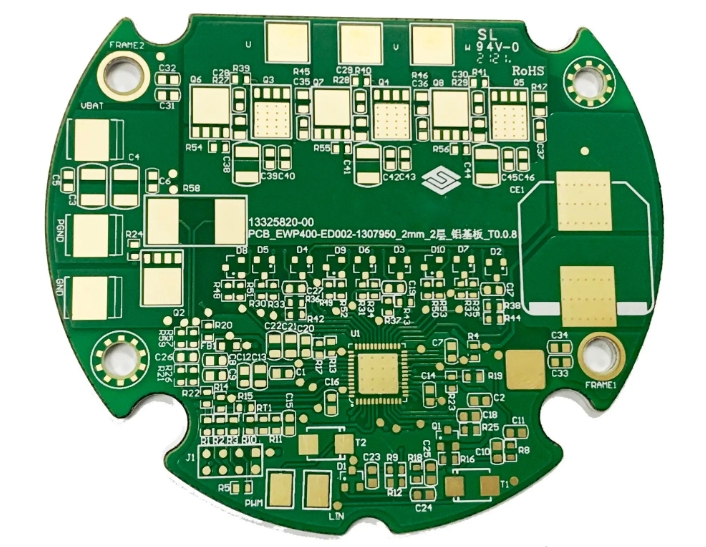
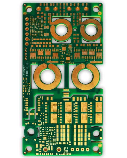
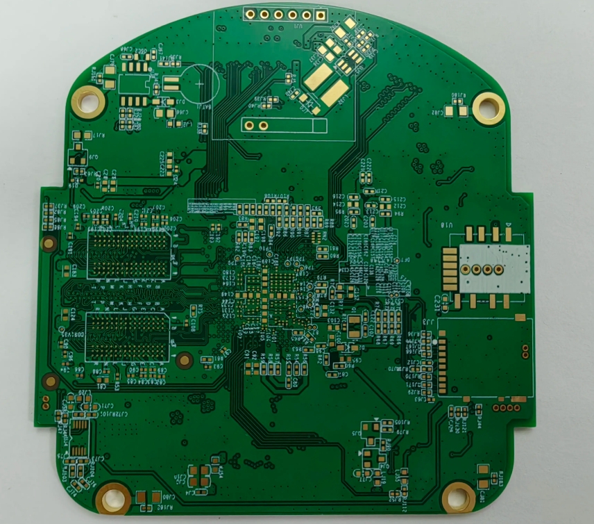
High-speed Printed Circuit Boards (HPC) have specific design requirements for high-speed signal transmission, high-frequency applications, and high-density layout. Compared with traditional PCBs, HPCs require more considerations during the design and manufacturing process, including signal integrity, electromagnetic compatibility, and thermal management.
High-Speed PCB Uses and Benefits
High-speed PCBs are circuit boards with high requirements in terms of signaling rate, frequency, and data transmission volume. They are widely used in communication, computer, aerospace, and other fields to meet the needs of high-speed signal transmission, high-frequency applications, and high-density layout.
Good high-frequency characteristics: The use of high-frequency materials, such as high-frequency boards and materials with low dielectric constants, effectively reduces signal attenuation and distortion.
Low Noise Characteristics: Reduce noise interference through shielding technology and grounding technology to ensure signal purity and stability.
High-density features: Microvia technology and multilayer board technology are adopted to realize higher integration and circuit density.
High-performance features: Impedance matching technology and signal integrity analysis technology are used to reduce signal reflection, crosstalk and attenuation, and improve signal integrity and stability.
Why is it important to have a PCB design process before proofing?
The reasons for the PCB design process before sampling mainly include the following aspects:
Ensure the feasibility of the design program: through the design phase, you can verify the circuit schematic and PCB layout design reasonableness, to ensure the feasibility of the design program in practical applications. If problems are found and modified during the design phase, bigger problems can be avoided during the sampling phase, thus saving time and cost.
Optimize wiring and component selection: In the design phase, designers can optimize the wiring design to reduce signal interference and transmission delays, and select appropriate components to ensure the performance and stability of the board. Proper wiring and component selection not only improve board performance but also reduce manufacturing difficulty and cost.
Reducing errors and omissions: Electrical connection errors or omissions can be minimized through rigorous review and testing during the design phase to ensure the integrity and correctness of the design. This helps avoid unnecessary modifications and rework during the prototyping process.
Compliance with design specifications: During the design process, it is necessary to follow the relevant design specifications, such as wiring width, spacing, aperture diameter, and so on. These specifications not only affect the performance of the circuit board, butare also related to the difficulty and cost of circuit board production. Following the specifications can ensure the quality and reliability of the board.
Prepare production files: After the design is completed, the design files need to be converted to the format required for production, including Gerber files, BOM sheets, drilling files, etc. These files are used for prototyping and production. These files are the basis for prototyping and production, ensuring a smooth production process.
High Speed PCB Design Guide
High-speed printed circuit board (PCB) design has become critical. Whether it’s a 5G device, a high-performance computer, or an IoT product, it needs to handle high-frequency signals. A poor layout can lead to signal distortion, electromagnetic interference (EMI) issues, and even system failure.
- Layered design
Layer design plays a very important role in high-speed circuits, just like a highway roadbed.
High-speed printed circuit boards, a reasonable layer structure is essential:
Use at least 4 layers (signal – ground – power – signal)
Ensure that critical signal layers are tightly coupled to adjacent planar layers
Consider using a symmetrical stacked layer structure to reduce warpage
Locate high-frequency signals in the inner layers to minimize radiation.
Remember: a good layer stack design can reduce signal integrity problems by more than 50%! - Impedance Control
Impedance mismatch is the enemy of high-speed board design:
Calculate and control microstrip and stripline impedance (typically 50Ω or 100Ω differential).
Confirm the board parameters (e.g. Dk value for FR4) with the PCB manufacturer.
Keep alignment width consistent to avoid sudden thinning
Differential pair alignment should be of strictly equal length (length difference <5mil)
Tip: Use tools such as SI9000 for impedance calculation, don’t just guess! - Power Integrity
High-speed circuits have extremely high power requirements:
Use low ESR/ESL decoupling capacitors (0402 package is better than 0603)
Follow the “large capacitors near the power supply, small capacitors near the chip” principle
Power plane division should be reasonable, to avoid the formation of “islands”.
Consider using power integrity simulation tools (e.g. HyperLynx PI).
Common mistake: thinking that the more capacitors the better improper layout is worse! - Signal routing techniques
High-speed signal alignment has special requirements:
3W principle: line spacing ≥ 3 times the line width
Avoid 90° corners (use 45° or arc instead)
Critical signals (e.g., clocks) should be prioritized
High-speed signals should not cross the plane division gap
Length matching is more important than you think! - The Art of Grounding
The grounding system is the “silent hero” of the high-speed printed circuit board:
Use multiple points of ground rather than a single point (more effective at high frequencies).
Avoid “ground loops” to form antennas.
Separate digital and analog grounds but do not completely isolate them
Leave an array of grounding vias under critical chips.
Remember: there is no perfect grounding scheme, only the one that best suits your design! - EMI control
Electromagnetic interference is the enemy of high-speed design:
Keep sensitive signals away from the board edge (≥20 mil).
Use grounded shielded vias to “fence” critical signals
Reduce reflections by choosing appropriate termination resistors
Consider using embedded capacitive materials
Fun fact: Many EMI problems stem from poor grounding design! - Design Verification
Final checklist:
After completing the DRC check, do another manual review
Request the impedance test report from the vendor
Do signal integrity simulations before small batch production.
Reserve test points for debugging
Lesson learned: a team skipped the simulation directly to mass production; the result is that 30% of the boards do not work!
Design Principles and Key Technologies
Signal Integrity (SI): High-speed PCB design requires control of transmission line impedance, termination impedance and differential impedance, and the use of special wiring strategies and termination matching techniques to reduce signal reflection and crosstalk.
Electromagnetic Compatibility (EMC): Shielding design, grounding design, and power management need to be considered in the design to reduce electromagnetic interference and ensure that the equipment works properly in an electromagnetic environment.
Thermal Management: High-speed PCBs generate heat during operation and require reasonable design of heat dissipation structures and materials to prevent overheating from affecting performance and reliability.
Material Selection
High-speed PCB is more stringent in material selection, usually using low loss, low dielectric constant and low dielectric loss factor of the board to ensure the stability and reliability of signal transmission.
Manufacturing Process
The manufacturing process of high-speed PCBs includes precise wiring, impedance control and surface treatment. For example, Shenzhen Xinhongxing Multilayer Circuit Co., Ltd. has applied for a patent involving a surface treatment device for high-density interconnected printed circuit boards, which greatly reduces air bubbles and realizes uniform coating using vibration and rotating motors, and tilting the guide seat to match the board’s self-rotation, to ensure a dense coating and stable electrical performance.
Scope of Application
High-speed printed circuit boards (high-speed PCBs) are used in a wide range of applications, including the following:
Data center switches: High-speed PCBs play an important role in data center switches, ensuring the integrity and stability of high-speed signal transmission and supporting the efficient operation of large-scale data centers.
AI servers: With the upgrading of AI servers and EGS platforms, the demand for high-speed PCBs has increased significantly. For example, the application of OAM boards, UBB boards, and CPU motherboards in AI servers is driving the high-speed PCB market.
Automotive Intelligence: In the field of automotive electronics, high-speed PCBs are used to realize the intelligent functions of automobiles, such as automatic driving and in-vehicle entertainment systems, to ensure the high performance and stability of automotive electronic systems.
Communication equipment: High-speed PCBs are widely used in communication equipment to support high-frequency, high-speed, and high-precision data transmission, ensuring signal integrity and low latency in the transmission process.
Computer Hardware: In high-end computer hardware, high-speed PCBs are used for high-performance computing and data processing, providing a stable and efficient data transmission path.
Medical Devices: High-speed PCBs are used in medical devices to ensure precise control and data transmission, improving the performance and reliability of medical devices.
Industrial Control: In the field of industrial control, high-speed PCBs are used to realize complex industrial control and data processing, ensuring stable operation and high efficiency of the system.