Table of Contents
What is the meaning of circuit board etching?
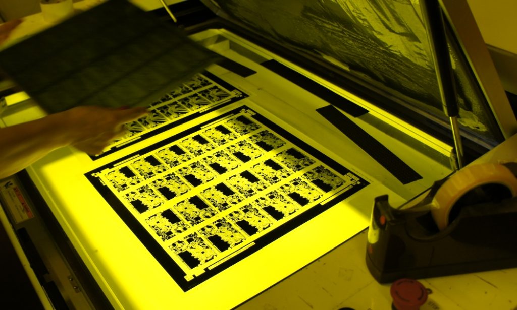
Circuit boards from the board to show the circuit graphics process is more complex, the current circuit board (PCB) processing of the typical process using the “graphic plating method”, that is, first in the outer layer of the circuit board to be retained on the part of the copper foil, that is, the circuit of the graphic part of a layer of lead and tin pre-plated on the corrosion-resistant layer, and then chemically corroded off the rest of the copper foil, called the Etching.
What is circuit board etching?
The etching method uses the etching solution outside the conductive lines of the copper foil removal method, the engraving method uses the engraving machine outside the conductive lines of the copper foil removal method; the former is a chemical method, more common, the latter is a physical method. The circuit board etching method is a chemical corrosion method that uses concentrated sulfuric acid to corrode unwanted copper cladding on circuit boards. The engraving method uses physical methods, with a specialized engraving machine, and the cutter head engraves copper-clad board to form a circuit alignment method.
Circuit board etching principle
The principle of PCB etching is the selective removal of unwanted copper foil from the copper-clad layer through chemical or physical methods, preserving the designed circuit pattern. The core of the process lies in redox reactions.
1. Basic Principle of Etching
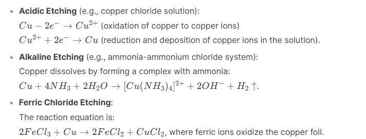
Etching involves using a chemical solution (etchant) to dissolve the unprotected copper foil areas through redox reactions, forming the desired circuit pattern. Key reactions include:
2. Classification of Etching Processes
- Wet Etching: Uses chemical solutions, divided into acidic (copper chloride) and alkaline (ammonia) types, suitable for high-precision circuits.
- Dry Etching: Relies on physical impact (e.g., plasma) to remove material, mainly used in semiconductor manufacturing.
3. Process Flow
- Pattern Transfer: The circuit design is transferred onto the copper-clad board via exposure/development or screen printing, forming a resist layer to protect the desired pattern.
- Etching: The board is immersed or sprayed with etchant to remove unprotected copper.
- Post-Processing: Resist stripping and cleaning yield the final circuit pattern.
4. Key Control Factors
- Etching Rate: Affected by solution concentration, temperature (typically 45±5°C), and flow rate.
- Undercut Control: Excessive etching time causes undercut; parameters must be optimized to improve the etch factor (ratio of etch depth to undercut width).
- Solution Maintenance: Regular replenishment of oxidizers (e.g., hydrochloric acid) ensures reaction efficiency.
The influencing factors of etching are as follows:
- Etching method
Soak and bubble etching will cause greater side corrosion, splash and spray etching side corrosion is smaller, especially spray etching the best results. - The type of etching solution
Different chemical components of different etching solutions, its etching rates is different, and the etching coefficient is also different. For example, the acidic copper chloride etching solution etching coefficient is usually 3, alkaline copper chloride etching solution etching coefficient can reach 4. Recent studies have shown that the nitric acid-based etching system can achieve almost no side etching to achieve the etching of the line sidewalls close to vertical. - Etching rate
The etching rate is slow will cause serious side corrosion, and etching quality improvement and etching rate have a lot to do with the acceleration. The faster the etching rate, the board stays in the etching solution to stay in the shorter the time, the smaller the amount of side corrosion, etching out the graphics clear and neat. - The pH value of the etching solution
The alkaline etching solution’s PH value is higher, and side corrosion increases. In order to reduce side corrosion, the general PH value should be controlled below 8.5. - Density of etching solution
Alkaline etching solution density is too low will aggravate the side corrosion; the choice of high copper concentration of etching solution to reduce the side corrosion is favorable. - Copper foil thickness
To achieve the minimum side corrosion of fine wire etching, it is best to use (super) thin copper foil. And the thinner the wire width, the thinner the copper foil thickness should be. Because the thinner the copper foil in the etching solution for the shorter pthe eriod, the smaller the amount of side corrosion.
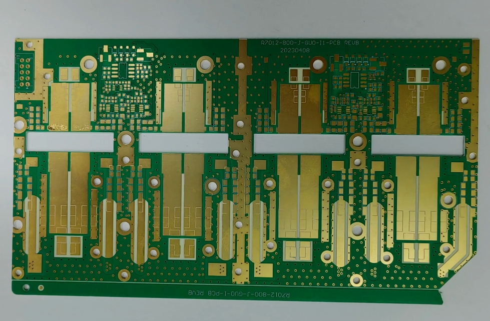
With the growing demand for miniaturization and high performance in electronic products, multilayer PCB boards have become the mainstream choice in the market by virtue of the higher integration, signal integrity, and heat dissipation performance they provide.
Etching Application Scope
Applications: Mainly used in PCB manufacturing (single-layer and multi-layer boards), semiconductor devices, etc.
Challenge: Need to balance etching accuracy and efficiency, to avoid residual copper or excessive etching caused by circuit defects.
Through the above principles and processes, etching technology realizes high-precision circuit graphic processing of electronic devices, which is one of the core processes of the modern electronics industry.