Solicitar presupuesto
NUESTRO BLOG
Céntrese en los artículos más recientes que cubren temas que van desde las últimas tecnologías a las mejores prácticas y noticias del sector para PCB.
2 de abril de 2026
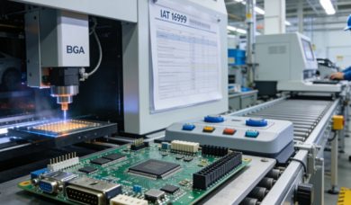
Elegir al proveedor adecuado de placas de circuito impreso ensambladas (PCBA) es fundamental para garantizar que su proyecto de electrónica cumpla los objetivos de calidad, coste y plazos. Este artículo analiza los factores que distinguen a los proveedores fiables, entre los que se incluyen la experiencia técnica, los sistemas de calidad, la selección de materiales, el control de procesos y la comunicación. Gracias a las recomendaciones prácticas y a las consideraciones basadas en casos reales, los ingenieros y los jefes de proyecto pueden tomar decisiones informadas a la hora de elegir proveedores.
24 de marzo de 2026
23 de marzo de 2026
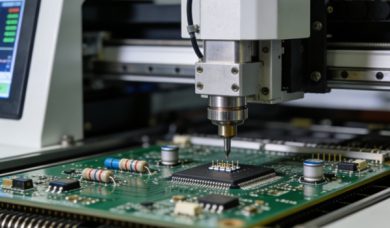
Este artículo explica los procesos de montaje especializados, las normas estrictas y las mejores prácticas para los PCB en sectores críticos como la electrónica médica, industrial, automotriz y aeroespacial.
25
Ene
El PCBA de alta mezcla y bajo volumen (HMLV) implica la producción de muchos diseños de PCB distintos en pequeñas cantidades. Ofrece una gran flexibilidad y personalización, pero se enfrenta a retos como la complejidad de la logística y la configuración. Ideal para I+D, prototipos y mercados especializados.
22
El montaje de PCB de bajo volumen sirve de puente entre la creación de prototipos y la producción en masa, y es ideal para tiradas limitadas. Ofrece soluciones flexibles y rentables con plazos de entrega habituales de entre 1 y 3 semanas. Este proceso permite realizar pruebas y validaciones de mercado.
20
Este artículo explica el montaje de prototipos de PCB, cubriendo su proceso, plazos de entrega típicos, factores de coste, métodos de prueba esenciales y mejores prácticas clave para garantizar el éxito de los prototipos de PCBA.
16
El montaje rápido de placas de circuito impreso permite crear prototipos y producir en poco tiempo, normalmente en unos días. Es ideal para proyectos urgentes, pero si se hace con prisas, la calidad puede verse afectada. Para ir rápido sin perder fiabilidad, necesitas socios expertos, procesos optimizados y archivos de diseño verificados.
13
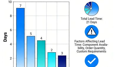
Este artículo explica los plazos de entrega habituales para el montaje de placas de circuito impreso (PCB) en prototipos y producción en serie. Detalla los factores clave que afectan al tiempo de entrega del montaje de placas de circuito impreso (PCBA) y ofrece estrategias prácticas para reducir los retrasos y acelerar los plazos de los proyectos.
08
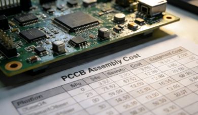
Descubra cómo se calculan los costes de montaje de placas de circuito impreso (PCB). Esta guía desglosa los factores clave: precios de los componentes, mano de obra, tarifas de pruebas y gastos generales. También ofrece estrategias prácticas para reducir eficazmente los gastos de montaje de placas de circuito impreso (PCBA) sin comprometer la calidad.
06
Conozca los archivos esenciales necesarios para un montaje eficiente de placas de circuito impreso. Los documentos clave incluyen archivos Gerber para las capas de circuitos, una lista de materiales (BOM) con todos los componentes y archivos Pick-and-Place para la programación automatizada de máquinas. Proporcionar estos documentos garantiza una producción rápida, precisa y de alta calidad de PCBA.
04
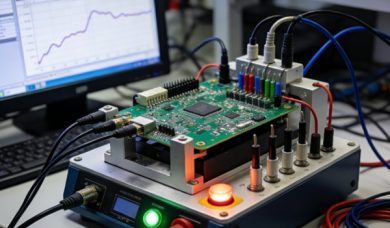
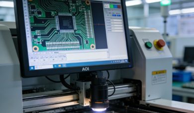
Este artículo explica los principales métodos de prueba de PCBA, como AOI, rayos X, ICT y pruebas funcionales. Explora cómo cada técnica detecta defectos, verifica la calidad del montaje y garantiza la fiabilidad del producto final. Descubra cómo estos métodos combinados protegen la fabricación de productos electrónicos.
02
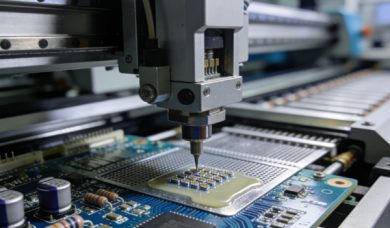
Este artículo compara los métodos de montaje de placas de circuito impreso SMT y THT. Analiza las diferencias clave en cuanto a coste, fiabilidad y aplicaciones típicas. SMT ofrece una mayor densidad de componentes y una mayor idoneidad para la automatización, mientras que THT proporciona uniones mecánicas más resistentes. El resumen ofrece orientación sobre cómo seleccionar la tecnología adecuada en función de los requisitos específicos del proyecto.
31
Dic
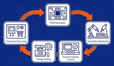
El montaje de placas de circuito impreso llave en mano es un servicio integral en el que un único proveedor gestiona todo el proceso, desde el abastecimiento de componentes hasta el montaje final y las pruebas. En esta guía se explica cómo funciona, destacando su eficacia a la hora de reducir tanto los costes de producción como los riesgos del proyecto mediante la consolidación de responsabilidades. Descubra por qué el montaje de placas de circuito impreso llave en mano es una solución optimizada para la fabricación de productos electrónicos.
29
TOPFAST ofrece soluciones integrales llave en mano para el montaje de placas de circuito impreso (PCB). Nuestros servicios abarcan el montaje SMT y THT, el abastecimiento de componentes (BOM), pruebas rigurosas y entrega rápida. Explore nuestros recursos para comprender el proceso de PCBA, la estimación precisa de costes y los plazos de entrega fiables.
26
Load More
Capas 1 Capa 2 capas 4 capas 6 capas 8 capas 10 capas 12 capas 14 capas
Dimensiones (mm)
Cantidad 5 10 15 20 25 30 35 40 50 75 100 100+
Espesor 0,4 mm 0,6 mm 0,8 mm 1,0 mm 1,2 mm 1,6 mm 2,0 mm 2,4 mm
Cantidad
Número de piezas únicas
Almohadillas SMT
Orificios pasantes