Designing Printed Circuit Boards (PCBs) is no easy task; it demands a blend of relevant knowledge, futuristic thinking, and a comprehensive understanding of the manufacturing process. This article is written with an intent to delve into the nuances and insights of PCB design, specifically focusing on maximizing efficiency keeping the fabrication process in mind. What aligns PCB Design with maximum efficiency? Are there any particular considerations that play a vital role in ensuring an efficient design? How can we design with a fabrication-first approach? How crucial is testing and validation in this context? These are the areas we will strive to shed light upon in this comprehensive guide. Whether you’re a beginner stepping into this realm, or an experienced professional aiming to enhance your knowledge, this article has insights that cater to a broad spectrum of readers. We will delve into intricate PCB Design fundamentals, discuss key considerations to be kept in mind for efficient designing, explore the depth of Design for Fabrication methodology and, at last, touch upon the significance of rigorous Testing and Validation. As we believe knowledge is power, let’s empower ourselves for creating and fabricating PCBs with maximized efficiency. Enjoy this enlightening journey of learning and discovery.

Table of Contents
PCB Design Fundamentals
At the foundation of designing PCBs for maximum efficiency lies a solid understanding of PCB Design Fundamentals. Therefore, let’s begin by demystifying the core principles central to this field. PCBs serve as the backbone of any electronic device, integrating different components and circuits in a compact way to enable intricate and complex functionalities. The design fundamentals encompass knowledge about component placement, wiring protocols, and layout strategies, among others. Specifically, understanding technicalities like circuit schematic, layer stacking, signal and power integrity, thermal management, shielding, and PCB assembly can significantly enhance the design output. What distinguishes an efficient design from an average one is the designer’s ability to interpret and apply these fundamentals according to the specific application at hand. This involves crafting a logical and intuitive layout that not only meets the circuit requirements but also simplifies manufacturing, while mitigating potential signal interference. Also, the ability to foresee fabrication challenges and accordingly optimise design to mitigate these is crucial within these fundamentals. By ensuring the design is robust and efficient from the outset, we can save valuable time, resources, whilst maintaining the integrity and reliability of the final electronic device. As we delve deeper in the following sections, each of these fundamental aspects will unfold to offer clear insights for efficient PCB designing.
Key Considerations for Efficient PCB Design
In the journey of crafting efficient PCB designs, a few key considerations stand paramount. First and foremost is the understanding of the end application – the ultimate use, necessity, and environment of the PCB. A clear comprehension of these factors will drive the selection of components, dictate the board size, and determine the power limitations. Then comes the selection of the right material suitable for the specific application, which can impact the overall performance and longevity of a PCB. Circuit complexity and board density are another essential aspects. Overcrowding can lead to heat accumulation, potentially decreasing the lifespan of components or causing system failure. Therefore, designers should consider the aspect of proper heat dissipation while designing. Component placement is a another crucial aspect; incorrect or inefficient placement can lead to errors during fabrication or operation. Lastly, ensuring the design meets industry standards is also vital. Incorporating industry standards in the design stage can streamline the fabrication process, reduce costs, and maintain product quality. It’s important to be mindful that efficiently designing a PCB is not merely about ensuring a functioning circuit, but also about working hand-in-hand with manufacturing and assembly requirements. This comprehensive understanding of key considerations can lead to the creation of better, more efficient PCB designs, inherently keeping fabrication easement in mind.

Design for Fabrication
In the realm of Printed Circuit Board (PCB) design, the concept of ‘Design for Fabrication’ (DfF) plays a colossal role. It denotes a framework of best practices and protocols focused on integrating manufacturing considerations right from the design phase. Rather than a conventional approach where design and fabrication exist as discrete silos, DfF embraces a prospective vision where these two aspects seamlessly blend. It implores designers to anticipate and understand the limits, capabilities, and nuances of the fabrication process, ensuring that any design they create is not merely an academic concept, but a realistic, manufacturable product. It sidesteps potential fabrication setbacks and revisions, thus saving both time and cost. Using DfF, the PCB design takes into account factors such as the type of material, optimal layout, minimum trace widths, hole sizes, surface finishes, and even manufacturer capabilities. By planning for these from the design phase, we ensure the PCB is designed not just for functionality, but for successful and efficient fabrication. Embracing DfF is crucial for an increasingly competitive electronics market. It paves the way for a smoother transition from design to production, reduces the risk of costly iterations, and ultimately culminates in a PCB that exhibits maximum efficiency and performance.
Testing and Validation
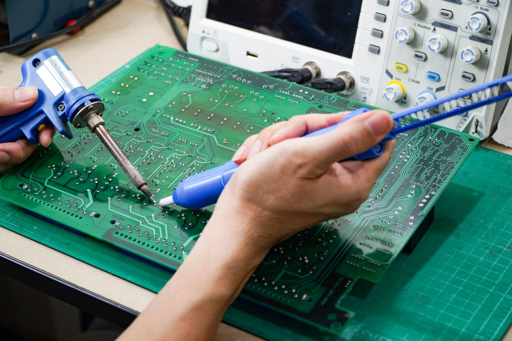
Testing and Validation inevitably form a crucial part of the PCB designing process, a stage that directly underpins the quality, safety, and effectiveness of the final product. It embraces a spotlight spotlight on identifying design flaws, component failures, or any inconsistencies that can potentially jeopardize the functionality or performance of the PCB. In essence, Testing and Validation is not just a mere phase; it is rather a relentless pursuit of perfection and reliability. These are not mere gatekeepers but tools that guide the transitions from design to fabrication and then to assembly, ultimately ensuring a product that not only resonates well with the set specifications but also provides reliable and long-term service. Different testing techniques such as in-circuit testing (ICT), functional testing (FCT), Automated Optical Inspection (AOI), and X-ray inspection are leveraged to ascertain the quality of the PCBs. Besides, the validation phase ensures that the PCB works as intended in its operating environment, thereby confirming its performance and adherence to required standards and conditions. Emphasizing on Testing and Validation helps in boosting the overall efficiency of the PCB, avoiding potential issues during fabrication, and saving both time and resources in the long run. Thus, it plays a cardinal role in creating PCBs underpinned by credibility and excellence.