Die Fertigungstoleranzen für Leiterplatten legen fest, wie viel Abweichung während des Herstellungsprozesses zulässig ist.
Sie wirken sich direkt aus auf Ertrag, Kosten, Zuverlässigkeit und Herstellbarkeit.
Viele Probleme mit Leiterplatten sind nicht auf mangelhafte Fertigung zurückzuführen, sondern auf Designs, die realistische Toleranzgrenzen überschreiten.
In diesem Leitfaden TOPFAST, ein professioneller Leiterplattenhersteller, erläutert die wichtigsten Toleranzen bei der Leiterplattenherstellung, ihre Auswirkungen auf die Produktion und wie Designer ein Gleichgewicht zwischen Leistung und Kosten herstellen können.
Inhaltsübersicht
Was sind Toleranzen bei der Leiterplattenherstellung?
Die Fertigungstoleranzen für Leiterplatten beziehen sich auf die zulässige Maß- und Prozessabweichungen die während der Herstellung auftreten.
Da die Leiterplattenherstellung chemische, thermische und mechanische Prozesse umfasst, Nullabweichung ist unmöglich.
Toleranzen definieren, welcher Grad an Abweichung als akzeptabel angesehen wird, ohne die Funktionalität oder Zuverlässigkeit zu beeinträchtigen.
Warum Toleranzen bei der Leiterplattenherstellung wichtig sind
Das Ignorieren von Fertigungstoleranzen kann zu folgenden Problemen führen:
- Geringe Produktionsausbeute
- Erhöhte Herstellungskosten
- Verzögerungen aufgrund von DFM-Überarbeitungen
- Zuverlässigkeit und Montageprobleme
Entwürfe, die mit den Fertigungsmöglichkeiten übereinstimmen, lassen sich einfacher, schneller und kostengünstiger produzieren.
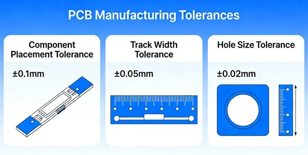
Wichtige Toleranzen bei der Leiterplattenherstellung, die Sie kennen müssen
Nachfolgend sind die wichtigsten Toleranzkategorien in der Leiterplattenfertigung aufgeführt.
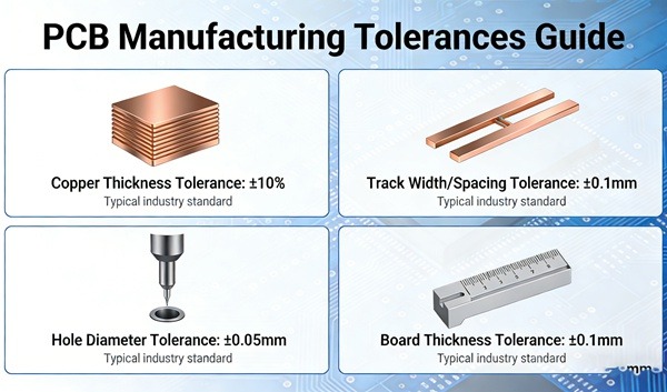
Spurbreite und Abstandstoleranz
Beschreibung:
Variation in der Breite und dem Abstand von Kupferbahnen, verursacht durch Ätz- und Belichtungsprozesse.
Warum es wichtig ist:
- Beeinflusst die aktuelle Kapazität
- Auswirkungen kontrollierter Impedanz
- Erhöht das Risiko von Öffnungen oder Kurzschlüssen
Design-Tipp:
Vermeiden Sie es, Leiterbahnen an absoluten Mindestgrenzen zu entwerfen, es sei denn, dies ist für die Leistung erforderlich.
Bohrungsgröße und Bohrtoleranz
Beschreibung:
Abweichung zwischen der geplanten Lochgröße und der Größe des fertigen plattierten Lochs.
Warum es wichtig ist:
- Beeinflusst die Passgenauigkeit der Komponenten
- Auswirkungen über die Zuverlässigkeit
- Beeinflusst die Beschichtungsqualität
Design-Tipp:
Berücksichtigen Sie immer die Größe des fertigen Lochs, nicht die Größe des Bohrers.
Toleranz des Ringes
Beschreibung:
Die minimale Kupferbreite um eine Bohrung herum.
Warum es wichtig ist:
- Verhindert Ausbrüche beim Bohren
- Sorgt für zuverlässige Durchkontaktierung
Design-Tipp:
Größere Ringringe verbessern die Ausbeute und Zuverlässigkeit erheblich.
Toleranz der Plattenstärke
Beschreibung:
Schwankungen in der Gesamtdicke der Leiterplatte nach der Laminierung.
Warum es wichtig ist:
- Auswirkungen der Impedanzsteuerung
- Beeinflusst die Kompatibilität der Anschlüsse
- Beeinflusst die mechanische Festigkeit
Design-Tipp:
Geben Sie die Dickentoleranz nur an, wenn dies erforderlich ist.
Ausrichtungstoleranz der Lötmaske
Beschreibung:
Fehlausrichtung zwischen Lötmaskenöffnungen und Kupferpads.
Warum es wichtig ist:
- Kann Spuren freilegen
- Verursacht Lötbrücken
- Beeinflusst die Montageausbeute
Design-Tipp:
Sorgen Sie für einen ausreichenden Abstand zwischen Lötmaske und Pads.
Toleranzen bei der Leiterplattenherstellung im Vergleich zu den Kosten
Engere Toleranzen erfordern mehr Prozesskontrolle, Inspektion und manchmal geringere Erträge.
| Toleranzstufe | Herstellungsschwierigkeit | Kostenauswirkungen |
|---|---|---|
| Standard | Low | Low |
| Mäßig | Mittel | Mittel |
| Eng | Hoch | Hoch |
Das Entwerfen mit unnötig engen Toleranzen erhöht oft die Kosten, ohne die Leistung zu verbessern.
Standard- vs. erweiterte PCB-Toleranzen
Nicht alle Leiterplatten erfordern denselben Toleranzgrad.
Standard-PCBs
- Unterhaltungselektronik
- Industrielle Steuerplatinen
- Stromversorgungen
Fortgeschrittene Leiterplatten
- HDI Entwürfe
- Digitale Hochgeschwindigkeitsschaltungen
- HF- und Mikrowellenplatinen
Fortgeschrittene Anwendungen erfordern engere Toleranzen, jedoch nur in kritische Bereiche, nicht über das gesamte Design hinweg.
Wie TOPFAST Toleranzen bei der Leiterplattenfertigung handhabt
Als professioneller Leiterplattenhersteller, TOPFAST kontrolliert Toleranzen durch:
- DFM-gesteuerte Designprüfung
- Prozessfähigkeitsanpassung
- Optimierung der Materialauswahl
- Statistische Prozesskontrolle
- Gezielte Inspektion bei risikoreichen Schritten
Dieser Ansatz gewährleistet eine stabile Qualität ohne unnötige Kostensteigerungen.
Wie Designer Toleranzen optimieren können
Um das beste Gleichgewicht zwischen Leistung und Herstellbarkeit zu erreichen:
- Entwerfen Sie auf Leistungsfähigkeit, nicht auf absolute Grenzen
- Toleranzen nur dort verschärfen, wo dies aus elektrischen Gründen erforderlich ist.
- Kommunizieren Sie wichtige Anforderungen klar und deutlich.
- Beziehen Sie den Hersteller frühzeitig in die Konstruktion ein.
Eine frühzeitige Zusammenarbeit spart oft später Zeit und Kosten.
Toleranzen bei der Leiterplattenherstellung und Montageertrag
Fertigungstoleranzen wirken sich direkt aus auf PCB-Montage Leistung:
- Eine Fehlausrichtung der Lötpaste erhöht Lötfehler
- Verformungen beeinträchtigen die BGA-Ausbeute
- Die Toleranz beeinflusst die thermische Entlastungsleistung.
Stabile Fertigungstoleranzen führen zu einer höheren Montageausbeute und weniger Ausfällen im Einsatz.
Schlussfolgerung
Die Fertigungstoleranzen für Leiterplatten definieren die Grenze zwischen einem herstellbaren und einem nicht herstellbaren Design.
Durch das Verständnis von Toleranzgrenzen und eine entsprechende Konstruktion können Ingenieure Kosten senken, die Ausbeute verbessern und eine zuverlässige Produktion sicherstellen.
Mit starkem DFM Unterstützung und kontrollierte Fertigungsprozesse, TOPFAST hilft Kunden dabei, das optimale Gleichgewicht zwischen Leistung und Herstellbarkeit zu erreichen.
Häufig gestellte Fragen (FAQ)
A: Produktionskosten steigen und Erträge sinken aufgrund von Prozessbeschränkungen.
A: Nein. Toleranzen sollten den funktionalen Anforderungen entsprechen und diese nicht unnötig überschreiten.
A: Einige Anpassungen sind möglich, aber größere Änderungen erfordern in der Regel eine Designänderung.
A: Nur für Parameter, die für die Leistung oder Montage entscheidend sind.