Angebot einholen
UNSER BLOG
Konzentrieren Sie sich auf die neuesten Artikel, die Themen von den neuesten Technologien bis hin zu Best Practices und Branchennachrichten für PCB abdecken.
März 18, 2026
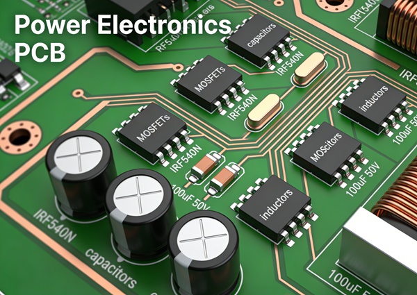
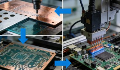
This article explores key design strategies for EV power electronics PCBs, including copper thickness selection, thermal management techniques, high-voltage spacing considerations, and stack-up optimization. It also discusses how PCB structure influences assembly reliability, particularly in high-power components and multilayer boards.
März 14, 2026
März 12, 2026
Dieser Artikel erläutert die Prototypenfertigung von Leiterplatten und behandelt dabei den Prozess, typische Vorlaufzeiten, Kostenfaktoren, wichtige Testmethoden und bewährte Verfahren, um erfolgreiche PCBA-Prototypen zu gewährleisten.
16
Jan.
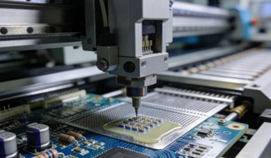
Die schnelle Leiterplattenbestückung ermöglicht eine rasche Prototypenentwicklung und Produktion, in der Regel innerhalb weniger Tage. Sie eignet sich für dringende Projekte, birgt jedoch Qualitätsrisiken, wenn sie überstürzt durchgeführt wird. Um Geschwindigkeit ohne Einbußen bei der Zuverlässigkeit zu erreichen, sind kompetente Partner, optimierte Prozesse und geprüfte Konstruktionsdateien erforderlich.
13
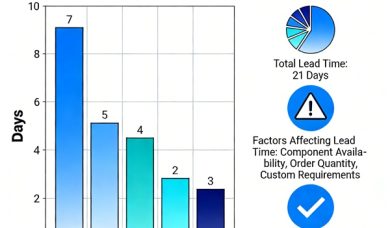
Dieser Artikel erläutert typische Vorlaufzeiten für die Leiterplattenbestückung bei Prototypen und der Massenproduktion. Er beschreibt wichtige Faktoren, die sich auf die Durchlaufzeit der Leiterplattenbestückung auswirken, und bietet praktische Strategien zur Reduzierung von Verzögerungen und zur Beschleunigung von Projektzeitplänen.
08
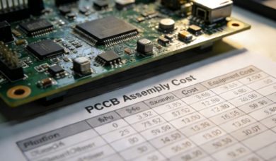
Erfahren Sie, wie die Kosten für die Leiterplattenbestückung berechnet werden. Dieser Leitfaden erläutert die wichtigsten Faktoren: Bauteilpreise, Arbeitskosten, Testgebühren und Gemeinkosten. Außerdem enthält er praktische Strategien, mit denen Sie Ihre PCBA-Kosten effektiv senken können, ohne Abstriche bei der Qualität machen zu müssen.
06
Lernen Sie die wesentlichen Dateien kennen, die für eine effiziente Leiterplattenbestückung erforderlich sind. Zu den wichtigsten Dokumenten gehören Gerber-Dateien für Schaltungsschichten, eine Stückliste (BOM) mit allen Komponenten und Pick-and-Place-Dateien für die automatisierte Maschinenprogrammierung. Die Bereitstellung dieser Dateien gewährleistet eine schnelle, genaue und qualitativ hochwertige PCBA-Produktion.
04
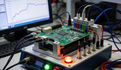
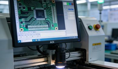
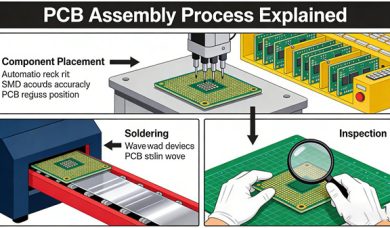
Dieser Artikel erläutert wichtige PCBA-Prüfverfahren wie AOI, Röntgen, ICT und Funktionsprüfungen. Er untersucht, wie jede Technik Fehler erkennt, die Montagequalität überprüft und die Zuverlässigkeit des Endprodukts sicherstellt. Erfahren Sie, wie diese kombinierten Verfahren die Elektronikfertigung schützen.
02
Dieser Artikel vergleicht SMT- und THT-Leiterplattenbestückungsverfahren. Er analysiert die wichtigsten Unterschiede in Bezug auf Kosten, Zuverlässigkeit und typische Anwendungsbereiche. SMT bietet eine höhere Komponentendichte und Eignung für die Automatisierung, während THT stärkere mechanische Verbindungen ermöglicht. Die Zusammenfassung enthält Leitlinien zur Auswahl der geeigneten Technologie auf der Grundlage spezifischer Projektanforderungen.
31
Dez.
Die schlüsselfertige Leiterplattenbestückung ist ein umfassender Service, bei dem ein einziger Anbieter den gesamten Prozess von der Beschaffung der Komponenten bis zur Endmontage und Prüfung übernimmt. In diesem Leitfaden wird erklärt, wie dies funktioniert, und es wird hervorgehoben, wie effizient dadurch sowohl die Produktionskosten als auch die Projektrisiken durch die Bündelung der Verantwortlichkeiten gesenkt werden können. Erfahren Sie, warum die schlüsselfertige Leiterplattenbestückung eine optimierte Lösung für die Elektronikfertigung ist.
29
TOPFAST bietet umfassende schlüsselfertige Lösungen für die Leiterplattenbestückung. Unsere Dienstleistungen umfassen SMT- und THT-Bestückung, Beschaffung von Bauteilen (BOM), strenge Tests und schnelle Lieferung. Informieren Sie sich über unsere Ressourcen, um mehr über den PCBA-Prozess, genaue Kostenvoranschläge und zuverlässige Lieferzeiten zu erfahren.
26
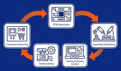
Dieser Artikel enthält eine Schritt-für-Schritt-Anleitung für den gesamten Prozess der Leiterplattenbestückung. Er behandelt wichtige Techniken wie SMT (Surface Mount Technology) und THT (Through-Hole Technology) sowie die erforderlichen Test- und Qualitätskontrollverfahren. Die Anleitung eignet sich sowohl für die Leiterplattenprototypenentwicklung als auch für die Serienfertigung und bietet einen klaren Überblick vom Bestücken der Bauteile bis zur abschließenden Überprüfung.
25
Lernen Sie die klaren Unterschiede zwischen der Leiterplattenherstellung und der Leiterplattenbestückung kennen. Bei der Herstellung wird durch Ätzen und Schichten die unbestückte Leiterplatte hergestellt, während bei der Bestückung (PCBA) diese mit Bauteilen bestückt wird. Sie unterscheiden sich in den Prozessen, Kostenfaktoren und Vorlaufzeiten. Letztendlich arbeiten diese aufeinanderfolgenden Phasen zusammen, um einen Entwurf in eine funktionsfähige Leiterplattenbaugruppe umzuwandeln.
22
Dieser umfassende Leitfaden zum HDI-PCB-Lagenaufbau behandelt alle Themen von den grundlegenden Konzepten bis hin zu fortgeschrittenen Anwendungen. Er beschreibt detailliert die strukturellen Eigenschaften, Konstruktionsprinzipien und Fertigungsaspekte für HDI-Leiterplatten verschiedener Stufen sowie häufig auftretende Probleme. Durch die Analyse der Konstruktionsspezifikationen für Blind-Vias, Strategien zur Optimierung der Zwischenlagen, Methoden zur Materialauswahl und Techniken zur Kostenkontrolle bietet er Elektronikingenieuren eine äußerst praktische und wertvolle technische Referenz.
19
Load More
Schichten 1 Lagen 2 Lagen 4 Lagen 6 Lagen 8 Lagen 10 Lagen 12 Lagen 14 Lagen
Abmessungen (mm)
Menge 5 10 15 20 25 30 35 40 50 75 100 100+
Dicke 0,4 mm 0,6 mm 0,8 mm 1,0 mm 1,2 mm 1,6 mm 2,0 mm 2,4 mm
Menge
Anzahl der Einzelteile
SMT-Pads
Durchgangslöcher