PCB is like the brain of an electronic product; once dirty, it will affect the performance of the whole machine. Improper cleaning can lead to four major problems: poor contact, component damage, circuit corrosion, and performance degradation. Unlike ordinary cleaning, PCB cleaning requires special tools and methods, just as cleaning antiques needs to be done extra carefully.
Table of Contents
Why must it be thoroughly cleaned?
In the manufacturing process of electronic products, welding residues left behind, like “invisible killer,” will bring three serious problems:
- Residual organic acids will gradually erode the circuit, like iron rust slowly damages your product.
- Invisible to the naked eye, conductive ions may lead to abnormal conduction of the circuit, there will be a short-circuit potential, resulting incause equipment failure.
- Residues will affect the appearance of the product; in a humid environment may produce a white mist, long term will lead to quality degradation.
Benefits of circuit board cleaning
- Prevents short circuits and electrical failures
Contaminants on circuit boards, such as solder paste, flux residue, dust, and grease, can lead to short circuits and electrical failures. By cleaning these contaminants, you can significantly reduce the risk of short-circuit and improve the reliability and stability of the circuit board. - Improve soldering quality
A clean board surface helps to improve the reliability of soldering joints and avoid poor soldering. The cleaning process removes soldering residues and ensures solder quality and connection reliability. - Improve thermal conductivity
Removing impurities such as thermal conductive media and adhesives improves the board’s thermal conductivity, protects electronic components, and ensures efficient heat dissipation. - Enhance appearance quality
Pollutants can affect the appearance quality of PCBA; the surface of the cleaned circuit board is smoother, avoiding the phenomenon of moisture absorption and whitening of residues. - Reduce the maintenance rate and improve product yields
After cleaning, the circuit board is cleaner, with no ionic pollution, effectively reducing the short circuit and signal interference caused by welding residues, product rework rate is reduced by more than 30%.
How to ensure the quality of PCB cleaning?
- Use specialized solvents for different residues.
- Strictly control the cleaning time, temperature, and process parameters.
- Use magnifying glass inspection, impedance test and other functional tests to ensure product quality.
- Control workshop temperature and humidity to prevent secondary pollution.
PCB cleaning process
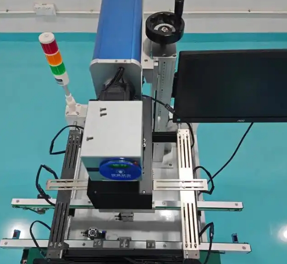
1. Full-automatic assembly line cleaning (mass production)
Workflow: chemical pre-wash → deep cleaning → multi-rinsing → high-pressure air knife dehydration → hot air drying
Core advantages
- Hundreds of circuit boards can be cleaned per hour.
- fully enclosed processing, avoiding manual contact
- stable and controllable cleaning effect
Applicable Scenarios
- Cell phone/computer motherboards and other high-volume production
- Automotive electronics with strict cleanliness requirements
2. Semi-automatic batch cleaning (small and medium batch)
Requires manual loading and unloading, can be flexibly configured in any part of the production line, needs to pay special attention to the placement angle and density of the circuit board to avoid incomplete or residual.
Core advantages
- Low investment cost of equipment
- can handle different sizes of PCBs and PCBAs
- Suitable for multi-species switching production
Applicable scenarios
- Industrial control equipment
- Medium and small batch medical electronic products
- R&D sampling stage cleaning needs
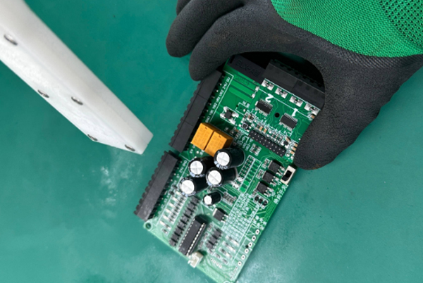
3. Manual cleaning (sample debugging special)
The use of a constant temperature cleaning tank requires cooperation with anti-static tools, key areas need to be manually reviewed.
Applicable scenarios
- experimental sample cleaning
- Rework veneer processing
- Special size board cleaning
4. Precautions
- must wear anti-static gloves
- Control the temperature of the cleaning solution (usually 50-60 ℃)
- Complex devices need to focus on checking
5. Cleaning process selection
- The mass production stage can be prioritized to choose fully automatic equipment
- pilot production stage recommended semi-automatic process
- R&D debugging, manual cleaning
- military/medical products recommended fully automatic + manual re-inspection
The correct cleaning process can not only improve the product’s appearance but also ensure the long-term stability of the circuit work, which is an important part of electronic manufacturing that can not be ignored. Each process has its applicable scenarios, the key is to choose the most economical solution according to the production demand, product characteristics, and quality requirements. Remember: not the most expensive equipment is the best, but the most suitable process is the best.
Circuit board cleaning methods
1. Physical cleaning method
- Ultrasonic deep cleaning
Like a sonic “bath”, the circuit board into a special cleaning solution, through which high-frequency sound waves generate millions of tiny bubbles. These bubbles rupture when the shock wave can penetrate every crevice, completely removing stubborn stains. It is especially suitable for cleaning hard-to-reach corners on high-density circuit boards. - High-pressure water gun rinsing
Adopting the principle of a high-pressure water gun similar to the car wash, by adjusting the water pressure and angle, quickly rinse a large area of the circuit board. This method is highly efficient and suitable for batch processing, but be careful to control the water pressure to avoid damage to precision components. - Soft brush cleaning
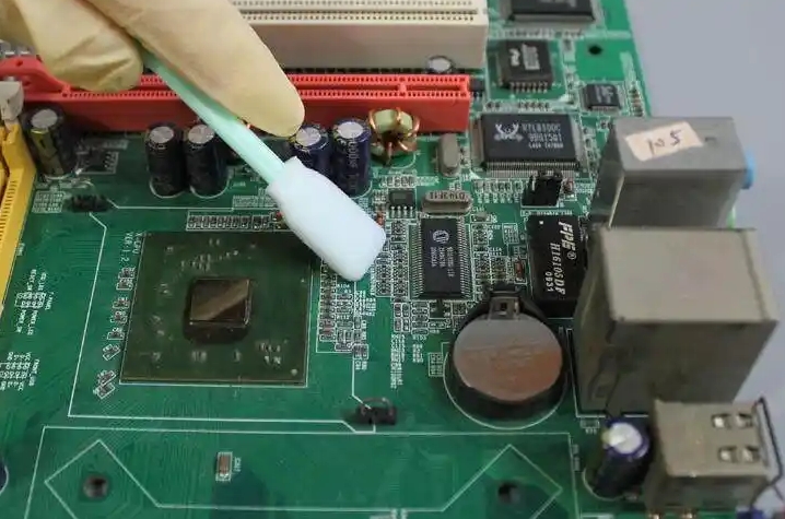
As gentle as brushing teeth, using a special anti-static brush with cleaning solution, suitable for removing surface dust and loose particles. Operation should be treated with the same care as precious works of art to avoid scratching the circuit.
2. Chemical cleaning method
- Solvent depth decontamination
The use of special electronic cleaners can quickly dissolve the oil and flux residues. Like the use of powerful stain remover, but need to pay attention to ventilation, because these solvents have a certain volatility. - Environmentally friendly water-based cleaning
The use of water-based environmental cleaning agents, adding special active ingredients. Both safe and economical, with an appropriate heating effect, is better. Like washing dishes with detergent, but using electronic special formulations.
Circuit board cleaning fluid
1. Flux-specific cleaning fluid
This type of cleaning fluid specializes in dealing with flux residues after soldering, as effectively as a cleaner that specializes in removing adhesive stains. Divided into two types:
Organic solvent-based: strong cleaning power, fast results, but the use of ventilation requires attention.
Water-based, environmentally friendly: safer and more environmentally friendly, but need to raise the temperature or extend the cleaning time.
2. Solder paste residue cleaning solution
Specially developed for solder paste, it can effectively decompose metal residues. Special attention should be paid when using:
Strictly control the soaking time (usually 3-5 minutes).
Maintain the appropriate temperature (recommended 50-60 ℃).
Rinse with deionized water immediately after cleaning.
3. Multi-functional all-purpose cleaning solution
This type of “all-purpose” cleaning solution is suitable for dealing with mixed pollution, characterized by:
Removes oil, dust, and light metal particles simultaneously.
Suitable for most common circuit board materials.
A small test area is recommended before use.
After cleaning, it is important to dry the board well and check the integrity of key components. The right choice of cleaning fluid not only improves cleaning efficiency but also protects the board from damage.
Conclusion: Circuit board cleaning is not an optional step, but a critical part of ensuring long-term product reliability. Just as surgical instruments must be sterilized, precision electronics must be thoroughly cleaned to ensure stable performance.