Table of Contents
What is a ceramic substrate?
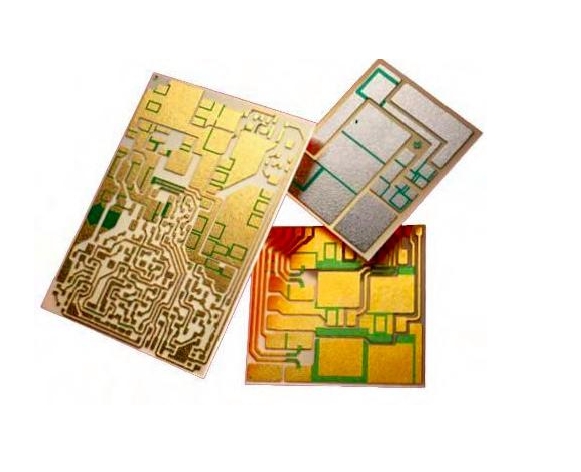
Ceramic substrate, also known as ceramic circuit board, is a ceramic material as a substrate, copper foil bonded to the surface of aluminum oxide (Al2O3) or aluminum nitride (AlN) ceramic substrate through high temperature (single-sided or double-sided) to form conductive lines and electronic components of the substrate. Compared with traditional organic substrates (such as FR-4), ceramic substrates have higher thermal conductivity, better mechanical strength, better high temperature, and corrosion resistance, so in the field of high-power, high-frequency, high-reliability electronic device packaging has irreplaceable advantages.
Advantages of the ceramic substrate
Strong mechanical stress, shape stability, specific high strength, high thermal conductivity, high insulation, strong bonding force, corrosion resistance, better thermal cycling performance, the number of cycles up to 50,000 times, high reliability, with the PCB board (or IMS substrate) as can be etched out of a variety of graphic structures; non-polluting, non-polluting, the use of a wide range of temperatures -55 ° C ~ 850 ° C; coefficient of thermal expansion is close to the silicon, to simplify the production process for power modules.
Common Ceramic Substrate Materials and Their Advantages
| Material | Advantages | Disadvantages | Applications |
|---|---|---|---|
| Alumina (Al2O3) | Low cost, high mechanical strength, good insulation properties, moderate thermal conductivity | Relatively low thermal conductivity | LEDs, power modules, automotive electronics |
| Aluminum Nitride (AlN) | High thermal conductivity, low thermal expansion coefficient, good insulation properties | High cost, difficult to process | High-power LEDs, lasers, microwave devices |
| Silicon Nitride (Si3N4) | High mechanical strength, low thermal expansion coefficient, excellent thermal shock resistance | High cost, relatively low thermal conductivity | High-temperature electronic devices, aerospace |
| Beryllium Oxide (BeO) | Extremely high thermal conductivity, good insulation properties | High cost, toxic | High-power microwave devices, aerospace |
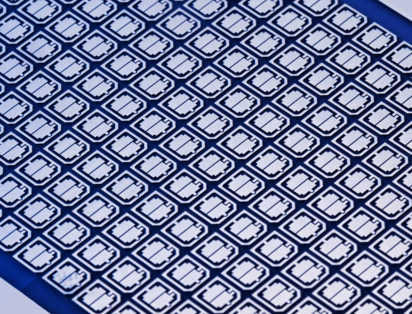
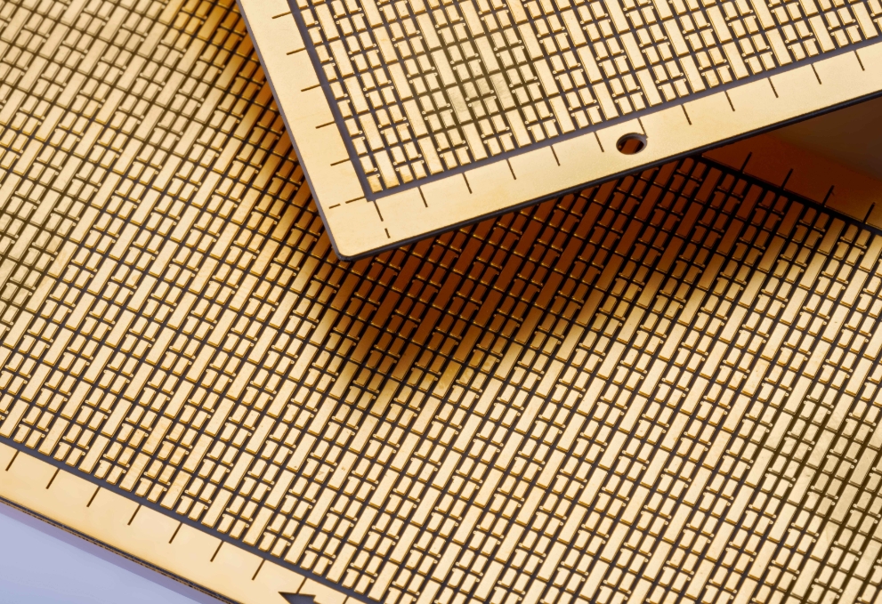
Ceramic substrate manufacturing process
The manufacturing process of ceramic substrate mainly includes the following:
Thin film process: the use of vacuum coating, photolithography, etching, and other processes in the formation of fine conductive lines on the ceramic substrate, suitable for high-density, high-precision circuits.
Thick film process: the use of screen printing, high-temperature sintering, and other processes in the formation of conductive lines on ceramic substrates, suitable for high-power, high-current circuits.
Direct Bonded Copper (DBC) Process: Copper foil is bonded directly to the ceramic substrate to form a high thermal conductivity, high-reliability circuit, suitable for high-power device packaging.
Active Metal Brazing (AMB) process: copper foil is brazed onto the ceramic substrate using active metal brazing material to form a high-strength connection, which is suitable for applications requiring high reliability.
Precautions
The ceramic substrate is a brittle material, in the processing and use of the process need to pay attention to prevent mechanical shock. Ceramic substrates of different materials have different coefficients of thermal expansion, in the design of circuits needs to take into account the thermal matching problem, you need to choose according to the actual application requirements.
Ceramic Substrates Application Areas
Ceramic substrates are widely used in the following fields:
LED Lighting: High-power LED chip packaging, improves heat dissipation efficiency and prolongs service life.
Power electronics: IGBT, MOSFET, and other power devices packaging, improve power density and reliability.
Automotive electronics: engine control modules, sensors, etc., to improve high temperature and vibration resistance.
Aerospace: high-reliability electronic device packaging to meet the requirements of the use of extreme environments.
Communication equipment: RF device, microwave device packaging, improve signal transmission efficiency.
With the rapid development of 5G communications, new energy vehicles, artificial intelligence, and other emerging industries, the growing demand for high-power, high-frequency, high-reliability electronic devices, the ceramic substrate as high-performance electronic packaging materials, its market demand will continue to expand, ceramic substrate industry will usher in a broader development prospect.