8
Feb
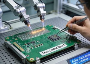
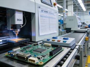
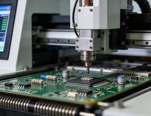
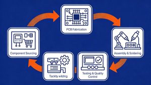
PCB Assembly vs Competitors: Which PCBA Manufacturer Is Right for You?
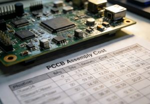
We compare TOPFAST against JLCPCB, PCBWay, and NextPCB in PCB assembly. Key factors include cost, lead time, quality, flexibility, and PCBA support, helping you choose...