Get a Quote
OUR BLOG
Focus on the latest articles that cover topics ranging from the latest technologies to best practices and industry news for PCB.
Apr 02, 2026
Selecting the right PCBA supplier is crucial for ensuring your electronics project meets quality, cost, and timeline goals. This article examines the factors that distinguish reliable suppliers, including technical expertise, quality systems, material selection, process control, and communication. With actionable how-to guidance and real-world considerations, engineers and project managers can make informed supplier decisions.
Mar 24, 2026
Mar 23, 2026
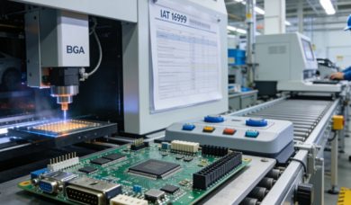
This article explains the specialized assembly processes, stringent standards, and best practices for PCBs in critical sectors like medical, industrial, automotive, and aerospace electronics.
25
Jan
High Mix Low Volume (HMLV) PCBA involves producing many distinct PCB designs in small quantities. It offers great flexibility and customization but faces challenges like complex logistics and setup. Ideal for R&D, prototyping, and specialized markets.
22
Low-volume PCB assembly bridges prototyping and mass production, ideal for limited runs. It offers flexible, cost-effective solutions with typical lead times of 1-3 weeks. This process supports testing and market validation.
20
This article explains prototype PCB assembly, covering its process, typical lead times, cost factors, essential testing methods, and key best practices to ensure successful PCBA prototypes.
16
Fast turn PCB assembly delivers rapid prototyping and production, typically within days. It suits urgent projects but risks quality if rushed. Achieving speed without sacrificing reliability requires expert partners, streamlined processes, and verified design files.
13
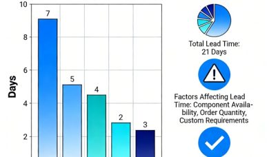
This article explains typical PCB assembly lead times for prototypes and mass production. It details key factors affecting PCBA turnaround time and provides practical strategies to reduce delays and accelerate project timelines.
08
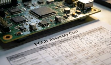
Learn how PCB assembly costs are calculated. This guide breaks down the key factors: component prices, labor, testing fees, and overhead. It also provides practical strategies to effectively reduce your PCBA expenses without compromising quality.
06
Learn the essential files required for efficient PCB assembly. Key documents include Gerber files for circuit layers, a BOM (Bill of Materials) listing all components, and Pick-and-Place files for automated machine programming. Providing these ensures fast, accurate, and high-quality PCBA production.
04
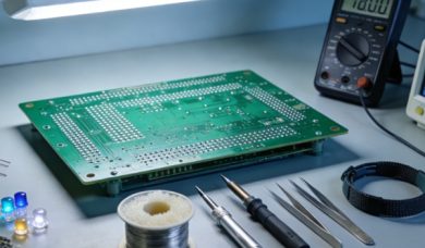
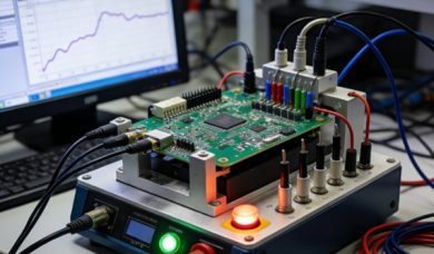
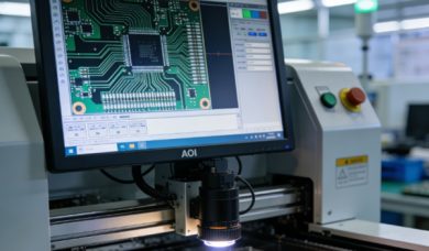
This article explains key PCBA testing methods like AOI, X-ray, ICT, and functional testing. It explores how each technique detects defects, verifies assembly quality, and ensures the final product's reliability. Learn how these combined methods safeguard electronics manufacturing.
02
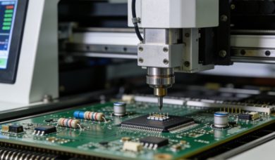
This article compares SMT and THT PCB assembly methods. It analyzes key differences in cost, reliability, and typical applications. SMT offers higher component density and automation suitability, while THT provides stronger mechanical bonds. The summary provides guidance on selecting the appropriate technology based on specific project requirements.
31
Dec
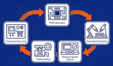
Turnkey PCB assembly is a comprehensive service where a single provider manages the entire process from sourcing components to final assembly and testing. This guide explains how it works, highlighting its efficiency in reducing both production costs and project risks by consolidating responsibilities. Learn why turnkey PCBA is a streamlined solution for electronic manufacturing.
29
TOPFAST delivers comprehensive turnkey PCB assembly solutions. Our services encompass SMT and THT assembly, component sourcing (BOM), rigorous testing, and rapid delivery. Explore our resources to understand the PCBA process, accurate cost estimation, and reliable lead times.
26
Load More
Layers 1 Layers 2 Layers 4 Layers 6 Layers 8 Layers 10 Layers 12 Layers 14 Layers
Dimensions (mm)
Quantity 5 10 15 20 25 30 35 40 50 75 100 100+
Thickness 0.4mm 0.6mm 0.8mm 1.0mm 1.2mm 1.6mm 2.0mm 2.4mm
Quantity
Number of Unique Parts
SMT Pads
Thru-Holes