Ball Grid Array (BGA) packages are widely used in modern electronics due to their high I/O density and compact footprint.
However, BGA solder joints are hidden beneath the package, making inspection and reliability management more complex than traditional leaded components.
Understanding how and why BGA solder joints fail is essential for long-term product stability.
This guide explains the most common BGA reliability risks, failure mechanisms, and inspection methods used in real production environments.
Table of Contents
Why BGA Reliability Is Critical
Unlike visible solder joints, BGA connections:
- Cannot be visually inspected after reflow
- Are sensitive to thermal stress
- Depend heavily on PCB flatness and stack-up stability
- Require controlled reflow and process management
Many assembly-related failures originate from fabrication instability.
For example, PCB warpage or layer imbalance during the PCB manufacturing process can increase BGA stress during thermal cycling.
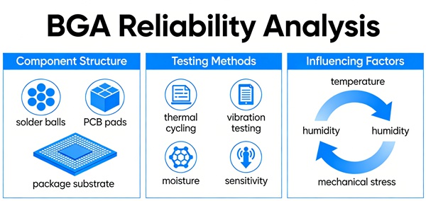
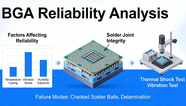
Common BGA Solder Joint Failure Mechanisms
1. Thermal Fatigue Cracking
The most common BGA failure mechanism is solder fatigue caused by repeated temperature cycling.
When devices heat up and cool down:
- The PCB expands
- The BGA package expands at a different rate
- Mechanical stress accumulates at the solder joint
Over time, micro-cracks form and propagate, eventually leading to open circuits.
2. Head-in-Pillow (HIP) Defects
Head-in-pillow occurs when the solder ball and solder paste fail to fully coalesce during reflow.
Causes include:
- Oxidation
- Warpage during reflow
- Improper temperature profile
HIP defects are often intermittent and difficult to detect without X-ray inspection.
3. Voiding in BGA Solder Joints
Voids are trapped gas pockets within the solder joint.
Excessive voiding can:
- Reduce thermal conductivity
- Increase electrical resistance
- Accelerate fatigue failure
Void percentage must be monitored according to IPC standards.
4. PCB Warpage and Assembly Stress
PCB flatness plays a major role in BGA reliability.
Boards with excessive warpage can:
- Cause uneven solder collapse
- Increase stress concentration
- Lead to early fatigue cracking
Fabrication tolerances influence this behaviour.
See: pcb manufacturing tolerances
5. Pad Cratering
Pad cratering occurs when the resin beneath a BGA pad fractures due to mechanical or thermal stress.
It is often associated with:
- Large BGA packages
- High Tg materials with poor adhesion
- Drop shock environments
Pad cratering is a board-level failure, not a solder issue.
Factors Affecting BGA Solder Joint Reliability
PCB Design Factors
- Copper balance
- Stack-up symmetry
- Via-in-pad structure
- Pad size and solder mask definition
Poor design choices can increase mechanical stress concentration.
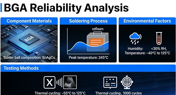
Reflow Profile Control
Proper reflow management ensures:
- Complete solder wetting
- Controlled temperature ramp
- Reduced oxidation
- Minimal warpage during heating
Excessive peak temperature or uneven heating increases stress risk.
Material Selection
Material CTE (Coefficient of Thermal Expansion) mismatch between:
- PCB substrate
- Solder alloy
- BGA package
directly influences fatigue life.
High-reliability applications often require optimised laminate selection.
Inspection and Failure Analysis Methods
Because BGA joints are hidden, specialised inspection tools are required.
X-ray Inspection
X-ray is used to detect:
- Voids
- Head-in-pillow defects
- Misalignment
It is a standard method in professional PCB assembly quality control
Cross-Section Analysis
Cross-sectioning allows engineers to:
- Observe crack propagation
- Measure plating thickness
- Analyse intermetallic layer growth
This is typically used for root cause analysis.
Thermal Cycling Testing
Accelerated life testing exposes boards to repeated temperature extremes to simulate long-term stress.
This helps estimate solder joint fatigue life.
How to Improve BGA Reliability
Practical recommendations:
- Maintain symmetric PCB stack-up
- Control copper distribution
- Use appropriate solder mask-defined pads when required
- Optimise the reflow temperature profile
- Monitor void percentage
- Avoid excessive PCB warpage
Early collaboration between design and manufacturing teams significantly improves BGA performance.
BGA Reliability in High-Reliability Applications
Industries such as:
- Industrial control
- Automotive electronics
- Aerospace systems
often require stricter inspection criteria and thermal cycling validation.
In these cases, process documentation and failure analysis capability are as important as the assembly itself.
Frequently Asked Questions (FAQ)
A: Thermal fatigue cracking due to repeated temperature cycling is the most common long-term failure mechanism.
A: No. Since joints are located under the package, X-ray inspection is typically required.
A: Yes. Thicker boards may resist warpage better, but stack-up balance and copper distribution are equally important.
A: Oxidation, warpage during reflow, and insufficient solder coalescence are common causes.
A: Improve stack-up symmetry, control reflow profile, reduce CTE mismatch, and verify solder joint quality through inspection and testing.
Conclusion
BGA solder joint reliability depends on a combination of PCB design, material selection, fabrication stability, and controlled assembly processes.
Understanding failure mechanisms such as thermal fatigue, voiding, and warpage allows engineers to reduce risk and improve long-term product performance.
BGA reliability is not only an assembly issue—it is a system-level engineering consideration that begins at PCB design and continues through manufacturing and quality control.