Table of Contents
Overview of Microvia Technology
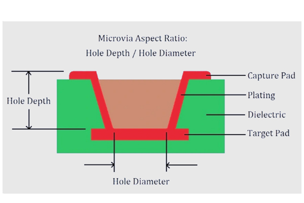
Microvia technology is a revolutionary breakthrough in modern printed circuit board (PCB) manufacturing, which realizes electrical connections between layers by drilling tiny holes with a diameter of less than 150 microns (about 6 mils) in the PCB. Compared with traditional mechanical drilling, microvia technology uses advanced processes such as laser drilling to achieve smaller hole diameters (up to 0.001mm) and higher precision processing.
The emergence of this technology has revolutionized the limitations of traditional PCB design, providing critical support for the miniaturization and high performance of electronic products. This technology not only significantly increases wiring density but also improves signal transmission performance, becoming the core manufacturing process for modern high-density interconnect (HDI) PCBs.
Core Benefits of Microporous Technology
Revolutionary increase in space utilization
The most notable advantage of microvia technology lies in its ability to dramatically enhance PCB wiring density. By using extremely small apertures, designers can arrange more circuits and components on the same board area. Taking smartphone motherboards as an example, after adopting microvia technology, the motherboard area can be reduced by 30%-50% while potentially doubling functionality. This space compression effect directly drives electronic products toward thinner and lighter designs.
Signal Integrity
In high-speed digital circuits and high-frequency analog circuits, signal transmission quality is paramount. Microvia technology significantly reduces signal attenuation and crosstalk by shortening interconnection paths (by more than 60% compared to traditional vias). Test data shows that for 10GHz high-frequency circuits using microvia technology, signal loss can be reduced by 15-20dB, which is decisive for applications such as 5G communication equipment and high-speed computing servers.
Dual Assurance of Reliability and Longevity
Microvia technology employs advanced materials and process controls, giving PCBs higher reliability and longer service life. By optimizing microvia structure and plating processes, thermal cycle life can be improved by 3-5 times. Tests on military-grade electronic products demonstrate that PCBs using microvia technology can withstand over 2000 extreme temperature cycles (-55°C to 125°C) without failure, far exceeding the 500-cycle standard of traditional PCBs.
Microporous Processing
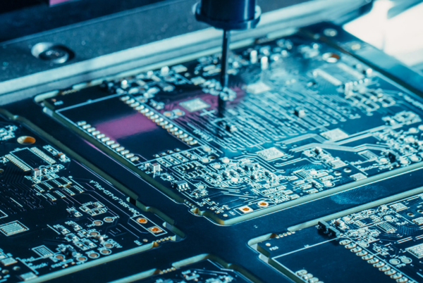
Laser Drilling
Laser drilling is currently the mainstream technology for microvia processing, primarily utilizing CO2 laser or UV laser systems. CO2 lasers are suitable for drilling holes of 50-150μm, while UV lasers can achieve smaller apertures (10-50μm). Modern laser drilling systems can achieve positional accuracy of ±5μm and drill over 5000 microvias per minute. However, laser energy control is critical—excessive energy can carbonize materials, while insufficient energy fails to penetrate, requiring precise parameter optimization.
Plating and Filling
The plating and filling process after microvia formation directly determines final quality. The mainstream approach combines “direct plating + pulse plating,” achieving complete void-free filling by optimizing additive formulations and current waveforms. Advanced horizontal pulse plating lines can control copper thickness uniformity within ±3μm and surface copper thickness variation to less than 10%, significantly improving reliability.
Comparative Advantages of Alternative Processes
Besides laser drilling, other microvia processing methods each have their own suitable applications:
- Photochemical Etching: Ideal for high-volume, high-precision planar microvia arrays, offering low cost but limited aspect ratio
- Microdrilling: Suitable for 0.1-0.3mm apertures with aspect ratios up to 15:1, but suffers from severe tool wear
- Electrical Discharge Machining (EDM): Effective for hard materials, but inefficient and costly
- Ion Etching: Capable of nanometer-scale microvias but requires substantial equipment investment
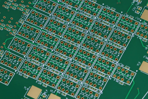
In-Depth Applications of PCB Microvia Technology
Design Specifications and CAD Implementation
Modern PCB design software (such as Cadence Allegro and Mentor Xpedition) incorporates specialized microvia design modules. Designers need to pay special attention to:
- Aspect ratio (recommended not exceeding 1:10)
- Safety spacing between microvias and circuits (typically ≥50μm)
- Alignment tolerance for stacked microvias (±25μm)
- Thermal design and current-carrying capacity calculations
The IPC-6012E and IPC-2226 standards provide detailed microvia design specifications, including acceptable quality criteria, testing methods, and reliability requirements.
Scientific Basis for Material Selection
Material selection for microvia PCBs is crucial. Common combinations include:
- High-frequency applications: Rogers RO4000 series + low-profile copper foil
- High-reliability applications: Isola 370HR + reverse-treated copper foil
- General consumer electronics: FR-4 standard materials + HVLP copper foil
Dielectric materials must have a low coefficient of thermal expansion (CTE), a high glass transition temperature (Tg), and excellent laser absorption characteristics. Copper foil surface treatment also directly affects laser drilling quality and hole wall smoothness.
Five Common Problems and Professional Solutions
Problem 1: Voids or Incomplete Filling in Microvia Plating
Root Cause Analysis:
Insufficient plating solution convection, additive imbalance, or improper current density can lead to filling defects. Higher aspect ratios increase filling difficulty.
Solutions:
- Adopt pulse reverse plating technology to enhance hole convection
- Optimize plating solution additive ratios to improve bottom deposition rates
- Use horizontal plating lines for better uniformity
- Control aspect ratio within 1:0.8
Problem 2: Positional Deviation in Laser Drilling
Root Cause Analysis:
Material inhomogeneity, laser focus drift, positioning system errors, or thermal deformation can cause drilling position deviations.
Solutions:
- Use UV laser + CCD vision positioning systems for ±3μm accuracy
- Add material pre-baking to reduce thermal deformation
- Regularly calibrate optical systems and motion platforms
- Employ high-precision materials (e.g., low-CTE substrates)
Problem 3: Microvia Fracture During Thermal Stress Testing
Root Cause Analysis:
CTE mismatch between copper (17ppm/°C) and substrate (FR-4: ~14-18ppm/°C x/y-axis, but 50-70ppm/°C z-axis) causes thermal cycle stress concentration.
Solutions:
- Select z-axis CTE-matched substrates (e.g., modified epoxy or polyimide)
- Optimize microvia taper (recommended 12-15 degrees)
- Use filled plating rather than tented plating
- Increase neck copper thickness (≥25μm)
Problem 4: Excessive High-Frequency Signal Loss Through Microvias
Root Cause Analysis:
Microvia structural discontinuities cause impedance mismatches, and rough hole walls increase skin effect losses.
Solutions:
- Use low-roughness reverse-treated foil (RTF<3μm)
- Optimize microvia size and position to match transmission line impedance
- Employ conductive paste filling to reduce loss
- For >10GHz applications, use back-drilling technology
Problem 5: Misaligned Stacked Microvias Causing Interconnection Failure
Root Cause Analysis:
Lamination shift, material shrinkage, or drilling positioning errors cause layer-to-layer microvia misalignment.
Solutions:
- Implement X-ray alignment systems (±10μm accuracy)
- Use dimensionally stable, low-shrinkage materials
- Design redundant connections (e.g., dual-microvia structures)
- Control lamination parameters (temperature gradient, pressure profile)
Industry Applications and Future Trends
Cross-Domain Innovative Applications
Microvia technology has demonstrated value across multiple high-end fields:
- 5G Communications: Millimeter-wave antenna arrays use microvias for high-density feed networks
- Artificial Intelligence: GPU/TPU chip packaging requires ultra-high-density microvia interconnects
- Medical Electronics: Implantable devices utilize microvia technology for miniaturization
- Automotive Electronics: ADAS systems rely on microvia PCBs for high reliability
Cutting-Edge Technology Directions
Microvia technology is evolving in several directions:
- Aperture Miniaturization: Progressing from 50μm to below 10μm
- 3D Integration: Stacked microvia layers advancing from 4-6 to over 10 layers
- Heterogeneous Integration: Combining different materials and aperture sizes on a single PCB
- Intelligent Inspection: AI-driven real-time microvia quality monitoring systems
Conclusio
As the core process of modern high-density electronic packaging, microvia technology has developed into a cross-disciplinary field integrating laser physics, electrochemistry, material science, and precision machinery. For PCB manufacturers, microvia technology is not only a reflection of production capacity but also a symbol of technical strength. The maturity of this technology directly determines the performance limit and reliability level of high-end electronic products.
From a practical point of view, the successful application of microvia technology requires the establishment of “design – materials – process – testing” four systematic solutions. Investment in advanced laser drilling equipment, the establishment of a perfect process control system.
At the same time, the concept of green manufacturing will promote the evolution of micro-hole processing in the direction of lower energy consumption and less pollution, which will help design more innovative and competitive products.