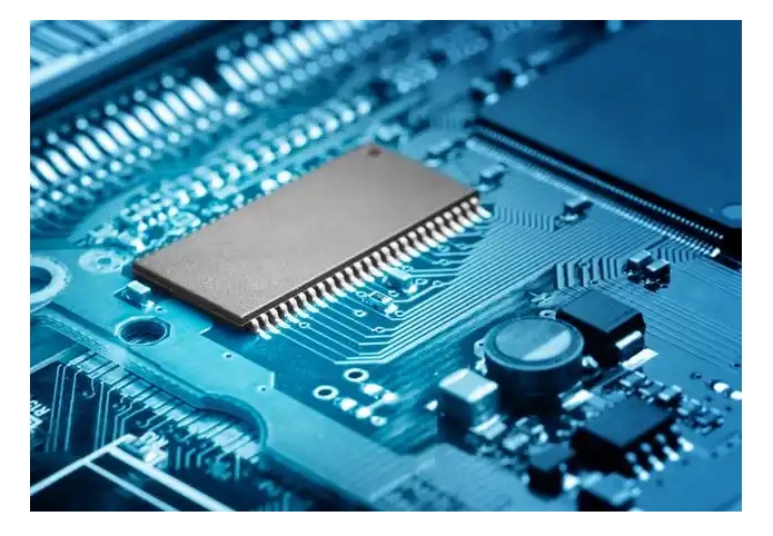
In today’s fast-paced electronics manufacturing industry, multilayer PCB prototyping must ensure quality while achieving rapid response and personalized customization to truly help customers seize market opportunities.
Table of Contents
Core Parameter Advantages
- Supports 2-32 layer prototyping, with minimum trace width/spacing of 2.5 mil.
- Minimum mechanical drill size: 0.15mm; laser microvia: 0.1mm.
- Materials include FR4 high-Tg laminates, halogen-free, and high-frequency/high-speed boards.
- Any-layer HDI technology: Supports ultra-high-density designs.
- High-precision automated production lines: Enhance processing accuracy from inner layer fabrication to surface finishing.
- Rapid prototyping channel: Expedited orders ship in as fast as 24 hours; standard prototyping in 3-5 days.
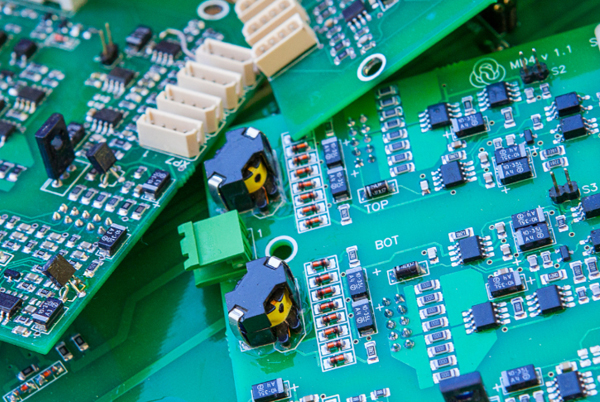
Applications
Widely used in consumer electronics, communication devices, medical electronics, automotive systems, and industrial automation, particularly critical for rapid validation of new product designs.
Conclusion
The perfect combination of fast prototyping and precision customization not only saves development time but also effectively reduces trial production risks. Choose Topfast to accelerate your innovation!
Topfast: Your Trusted PCB Manufacturing Partner Since 2008
Founded in 2008, Topfast is a global leader in PCB design, manufacturing, and assembly with 17 years of experience. As a one-stop PCB solution provider, we specialize in rapid prototyping and small-batch production for clients worldwide. With over 1,000 employees and a 20,000-square-meter factory, we have served prestigious companies such as Huawei, Xiaomi, Rakuten, Thales Group, Mitsubishi, DJI, Hikvision, and various global IoT enterprises.
Our commitment to high quality and on-time delivery has earned us widespread acclaim in the industry. We remain dedicated to customer satisfaction, delivering both “high quality” and “fast turnaround” to become a trusted PCB service provider.
Adhering to a customer-first, quality-driven philosophy, we provide diversified customization services to meet user demands, ensuring win-win collaboration while minimizing costs and maximizing production efficiency.
5 Common PCB Multilayer Prototyping Issues & Solutions (Q&A)
Q1: How to ensure interlayer alignment accuracy in multilayer PCBs?
Issue: Layer misalignment during lamination can lead to poor conductivity.
Solution:
- Use high-precision alignment systems (±25μm accuracy).
- Implement X-ray drilling positioning technology.
- Include optical alignment markers in the design.
- Recommend maintaining a sufficient alignment margin (≥0.2mm).
Q2: What special considerations apply to high-frequency PCB prototyping?
Issue: Poor material or design choices can degrade signal integrity.
Solution:
- Use specialized high-frequency laminates (Rogers, Taconic).
- Strict impedance control (provide detailed stack-up requirements).
- Avoid 90° turns—use curved or 45° traces.
- Offer signal integrity analysis reports (optional).
Q3: How to address microvia (blind/buried via) processing challenges in HDI PCBs?
Issue: Rough via walls or uneven copper plating in microvias.
Solution:
- Utilize laser drilling (CO2/UV laser).
- Apply pulse plating for uniform copper thickness.
- Recommend microvia size ≥0.1mm, aspect ratio ≤0.8:1.
- Provide cross-section analysis for quality verification.
Q4: How to balance speed and quality in fast-turn prototyping?
Issue: Expedited orders may compromise quality control.
Solution:
- Dedicate separate rapid prototyping production lines.
- Implement parallel engineering (design review + material prep).
- Maintain standard material inventory (e.g., FR4 common thicknesses).
- Apply full inspection standards even for fast-turn orders.
Q5: How to reduce costs for small-batch prototyping?
Issue: High per-unit costs strain development budgets.
Solution:
- Offer panel-sharing services (multiple customers on one panel).
- Recommend standard parameters (1oz copper, green solder mask).
- Optimize the design upfront to minimize revisions.
- Establish long-term partnerships for volume discounts.
More Reading Recommendations
Multilayer PCB Blind Hole Process
Multilayer PCB Vs High Speed and High Frequency PCBs
Multi-layer PCB Design and Production
PCB Manufacturing Proofing Process