PCB drilling is a critical step in printed circuit board manufacturing, directly impacting the board’s electrical performance and mechanical strength. This article provides an in-depth exploration of various PCB drilling technologies, key process considerations, and practical solutions to common production issues.
Table of Contents
Overview of PCB Drilling Technology
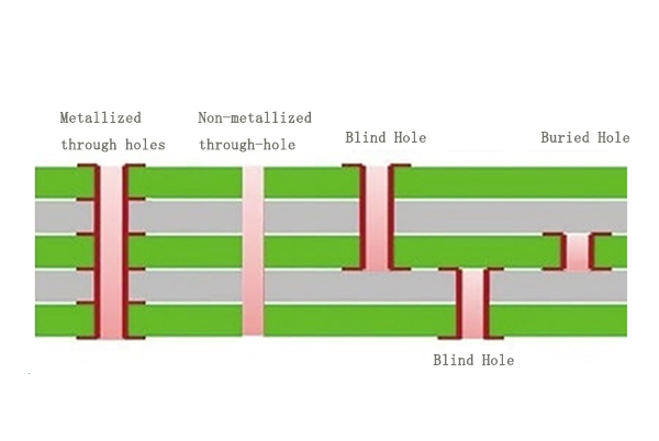
The primary purpose of PCB drilling is to create holes for electrical connections and component mounting. Based on design requirements, PCB holes are categorized into three main types:
- Through-Holes: Penetrate the entire board, used for connecting different layers or mounting through-hole components.
- Blind Vias: Extend from the outer layer to an inner layer without passing through the entire board.
- Buried Vias: Located entirely between inner layers and not visible on the surface.
As electronic devices trend toward miniaturization and high-density designs, blind and buried vias are increasingly used in HDI (High-Density Interconnect) boards.
Main PCB Drilling Methods
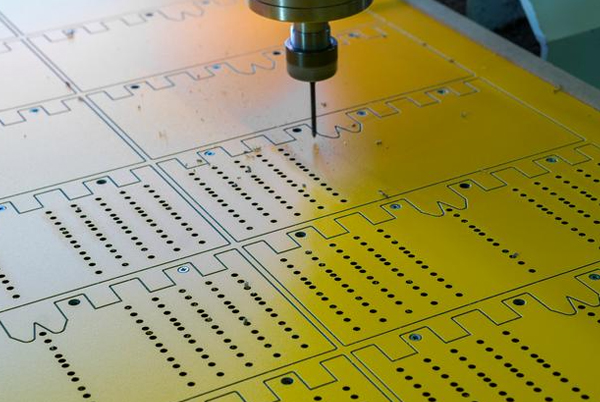
Mechanical Drilling
Mechanical drilling is the most common method in PCB manufacturing, especially for through-holes:
- Drill Bit Material: Typically carbide (tungsten carbide) bits with diameters ranging from 0.1mm to 6.5mm.
- Spindle Speed: High-speed spinners can reach 150,000–200,000 RPM.
- Positioning Accuracy: Modern CNC drilling machines achieve ±25μm precision.
- Panel Stacking: Typically, 2–3 PCBs are stacked for simultaneous drilling to improve efficiency.
Key factors include drill bit selection and maintenance. Worn bits cause rough hole walls and dimensional deviations, requiring regular replacement. Additionally, feed rate and spindle speed must be optimized based on material type and thickness.
Laser Drilling
Laser drilling is ideal for microvias and HDI boards:
- CO₂ Lasers: Wavelength of 10.6μm, mainly for non-metal materials like FR-4 substrates.
- UV Lasers: 355nm wavelength, capable of directly drilling copper layers, suitable for microvias.
- Precision: Can create 50–150μm diameter microvias.
- Speed: Capable of drilling hundreds to thousands of holes per second.
Advantages include non-contact processing (no mechanical stress) and the ability to create high-aspect-ratio microvias unachievable with mechanical drilling. However, equipment costs are high, and copper thickness limitations apply.
Other Specialized Drilling Methods
For specialized applications, alternative methods include:
- Plasma Etching: Uses plasma chemical reactions to remove material, suitable for high-aspect-ratio microvias.
- Chemical Etching: Forms holes via chemical dissolution, mainly for special materials.
- Hybrid Mechanical-Laser Drilling: Combines both technologies for improved efficiency and quality.
Key Considerations in PCB Drilling
Pre-Drilling Preparation
- Material Selection & Conditioning: Different substrates (FR-4, high-frequency materials, flex PCBs) require different drilling parameters. Ensure boards are thoroughly dried to prevent moisture-related defects.
- Drill Bit Selection & Management: Choose appropriate bits based on hole size and material. Track bit usage and replace worn bits promptly.
- Parameter Optimization: Adjust spindle speed, feed rate, and retract speed based on material properties. Harder materials require slower feeds, while softer materials allow higher speeds.
In-Process Quality Control
- Hole Position Accuracy: Regularly calibrate equipment and use high-precision positioning systems (e.g., linear encoders).
- Hole Wall Quality: Ensure smooth walls free of burrs or “nail heads.” Inspect via microscopy or AOI (Automated Optical Inspection).
- Chip Removal: Effective debris extraction prevents recutting. Maintain vacuum systems to clear chips promptly.
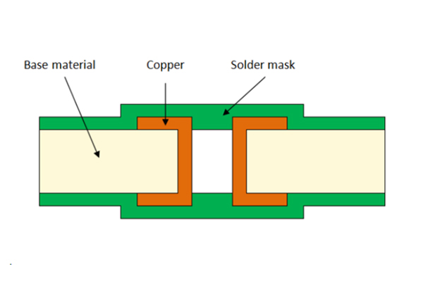
Post-Drilling Processes
- Deburring: Remove edge burrs chemically or mechanically to improve smoothness.
- Copper Deposition & Plating: Electroless and electrolytic copper plating establish conductive layers for interconnects. Control bath chemistry and plating parameters strictly.
- Solder Mask Application: Coat non-solder areas to protect hole walls and prevent shorts.
Common PCB Drilling Issues & Solutions
Issue 1: Drilled Hole Position Deviations
Causes:
- Poor equipment calibration or low positioning accuracy.
- Panel movement during drilling.
- Excessive drill bit wear is causing deflection.
Solutions:
- Calibrate drilling machines regularly.
- Improve panel fixation (vacuum suction or mechanical clamping).
- Implement a bit replacement schedule.
- For high-precision needs, consider laser drilling.
Issue 2: Rough Hole Walls with Burrs or Resin Residue
Causes:
- Worn bits or incorrect parameters.
- Challenging materials (e.g., high-Tg substrates).
- Poor chip evacuation is causing recutting.
Solutions:
- Optimize drilling parameters (speed, feed rate).
- Use specialized bits for difficult materials.
- Enhance chip extraction.
- Add a deburring step if necessary.
Issue 3: Difficulty Drilling Microvias (≤0.2mm), High Breakage Rate
Causes:
- Insufficient micro-bit strength.
- Suboptimal parameters.
- Hard or impure materials.
Solutions:
- Use high-quality micro-bits with minimal overhang.
- Optimize parameters (higher speed, lower feed).
- Switch to laser drilling where feasible.
- Pre-drill pilot holes for guidance.
Issue 4: Poor Inner-Layer Copper Connection to Hole Walls
Causes:
- Rough hole walls from poor drilling.
- Improper electroless copper parameters.
- Inadequate inner-layer surface preparation.
Solutions:
- Improve drilling quality for smoother walls.
- Optimize pre-plating treatments (desmear, activation).
- Adjust electroless copper bath chemistry.
- Apply plasma treatment for better wettability.
Issue 5: Degraded Dielectric Performance in High-Frequency Boards
Causes:
- Thermal damage during drilling.
- Signal reflections from rough walls.
- Contamination affecting material properties.
Solutions:
- Use sharp bits with optimized cooling.
- Consider laser drilling to reduce mechanical stress.
- Improve post-drill cleaning.
- Apply back-drilling to minimize stub effects.
Issue 6: Incomplete Blind Via Penetration
Causes:
- Inconsistent laser energy control.
- Uneven dielectric thickness.
- Insufficient inspection methods.
Solutions:
- Fine-tune laser energy and pulse settings.
- Tighten dielectric layer thickness control.
- Implement blind via bottom inspection.
- Adopt advanced methods like infrared inspection.
Future Trends in PCB Drilling
As electronics demand higher density and frequency, drilling technology continues evolving:
- Smaller Holes: From standard 0.3mm to 0.1mm or smaller for HDI needs.
- Higher Precision: Positioning accuracy improving from ±50μm to ±15μm or better.
- Hybrid Techniques: Combining mechanical and laser drilling for optimal results.
- Smart Manufacturing: AI-driven parameter optimization and real-time monitoring.
- Eco-Friendly Processes: Reducing waste and hazardous materials.
Conclusion
PCB drilling is a pivotal process that significantly impacts product reliability. Understanding various drilling methods, troubleshooting common issues, and staying updated on advancements are essential for quality PCB production. As technology progresses, drilling will become more precise, efficient, and intelligent, supporting next-generation electronics.