Table of Contents
Classification of Electroplating Processes
Acid Bright Copper Plating, Nickel Plating, Gold Plating, Tin Plating
Process Flow
- Acid Dip →
- Panel Plating (Copper) →
- Pattern Transfer →
- Acid Cleaning →
- Two-Stage Countercurrent Rinsing →
- Microetching →
- Two-Stage Countercurrent Rinsing →
- Acid Dip →
- Tin Plating →
- Two-Stage Countercurrent Rinsing →
- Acid Dip →
- Pattern Copper Plating →
- Two-Stage Countercurrent Rinsing →
- Nickel Plating →
- Two-Stage Water Rinsing →
- Citric Acid Dip →
- Gold Plating →
- Recovery Rinse →
- 2-3 Stage DI Water Rinsing →
- Drying
(Note: “Countercurrent rinsing” refers to a water-saving rinsing method where fresh water flows opposite to the workpiece movement.)
1. Acid Dipping
- Purpose
- Remove surface oxides and activate the panel
- Sulfuric acid concentration: 5%-10% (prevents dilution-induced instability)
- Key Controls
- Time: Avoid excessive dipping to prevent oxidation
- Maintenance: Replace when turbid or copper content exceeds 20g/L
- Chemical: Use CP-grade sulfuric acid
2. Panel Plating (Primary Copper Plating)
- Purpose
- Protect thin electroless copper deposits from oxidation/etching
- Process Parameters
- High-acid, low-copper formula (H₂SO₄: 180-240g/L, CuSO₄: 75g/L)
- Additives: Chloride ions (brightener aid), copper brightener (3-5ml/L initial dose)
- Current density: 2A/dm² (Calculation: Panel length × width × 2 × 2A/dm²)
- Temperature: 22-32°C (cooling system recommended)
- Maintenance
- Daily: Brightener replenishment (100-150ml/KAH), filter pump checks
- Weekly: Composition analysis (CuSO₄/H₂SO₄/Cl⁻), Hull cell testing
- Monthly: Anode basket cleaning, carbon filtration (6-8 hrs)
- Annual: Carbon treatment (as needed)
- Major Treatment Procedure
- Anode prep: Micro-etching → Alkaline/acid soaking
- Bath treatment: H₂O₂ oxidation → Carbon adsorption → Filtration → Electrolysis
- Parameter adjustment: Restore H₂SO₄/CuSO₄/Cl⁻ levels
3. Acid Cleaning
- Purpose
- Remove oxides/residues to ensure adhesion for pattern plating
- Acid (not alkaline): Prevents resist damage
- Controls
- Concentration: 10%
- Time: ≥6 minutes
- Bath life: 15m²/L working solution
4. Microetching
- Purpose
- Roughen copper surface for improved bonding
- Parameters
- Etchant: Sodium persulfate (60g/L)
- Time: 20 sec
- Copper limit: <20g/L
5. Pattern Copper Plating
- Purpose
- Build up copper thickness for current-carrying capacity
- Process
- Same as panel plating
6. Tin Plating
- Purpose
- Serve as etch resist for circuitry
- Parameters
- Bath: Stannous sulfate (35g/L), H₂SO₄ (10%)
- Current density: 1.5A/dm²
- Temperature: 22-30°C (cooling required)
- Maintenance
- Regular analysis, anode bag cleaning, carbon treatment
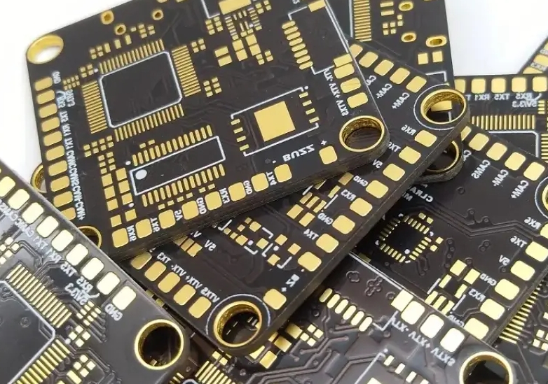
7. Gold Plating
- Types & Purpose
- Hard gold (Ni/Co alloy): Wear resistance
- Soft gold (pure): Solderability
- Parameters
- Citrate-based bath: Au 1g/L, pH 4.5, 35°C
- Pre-treatment: Citric acid dip to minimize contamination
- Critical Controls
- Anode: Platinum-coated titanium (avoid stainless steel)
- Post-treatment: Alkaline dip to prevent oxidation
8. Nickel Plating
- Purpose
- Barrier layer against Cu/Au diffusion; enhances mechanical strength
- Parameters
- Current density: 2A/dm²
- Temperature: 50°C (heating required)
- Maintenance
- Regular replenishment of nickel sulfamate/chloride and boric acid
- Anode nickel pellets require surface roughening
Critical Notes
- Safety: Incremental H₂SO₄ addition to avoid thermal runaway
- Precision: Chloride dosing (30-90ppm) requires exact measurement
- Contamination Control: Carbon treatment + low-current electrolysis
This standardized process ensures uniform plating thickness, adhesion, and reliability.
