As the electronics industry continually evolves, so does the demand for flexible and efficient printed circuit boards (PCBs). The central player in this domain is Flex PCB; renowned for its adaptability, durability, and substantial contribution towards miniaturization in electronics. Whether you’re a seasoned designer or just venturing into the electronics field, getting your Flex PCB design right is a crucial step towards achieving optimal performance and product durability. This comprehensive guide delves into the intriguing world of Flex PCBs, their integral role in the ever-progressing electronics industry, and above all, the ‘7 Must-Knows’ for a successful Flex PCB design. We will break each element down, from understanding the tight bend radius to grasping the critical function of stiffeners, the necessity of specialized materials, and more. Welcome aboard this illuminating journey into the intricate nuances of Flex PCB design and yield a rewarding design experience like never before.
Table of Contents
Understanding Flex PCB Design
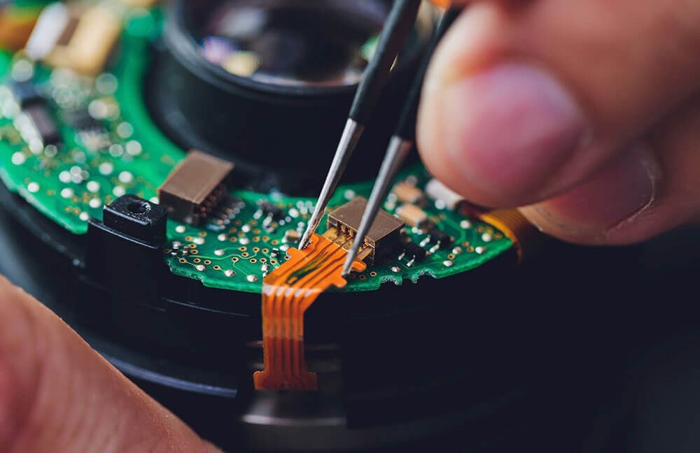
Flex PCB, or Flexible Printed Circuit Board, is a highly adaptable type of PCB that offers special benefits for many modern electronic applications. Unlike a conventional PCB made with rigid fiberglass material, Flex PCB leverages flexible plastic substrates like polyimide. This flexibility allows for the production of electronic assemblies with tight bends and complex geometries that simply cannot be achieved with standard PCBs. As such, Flex PCB is a game-changer in the electronic industry, paving the way for miniaturized devices and tackle space constraint issues. It is widely utilized in everything from everyday consumer electronics to advanced aerospace and medical equipment. Understanding the complexity and potential of Flex PCB design is integral for engineers and manufacturers alike, as this knowledge can largely impact the efficiency, reliability, and space utilization in various electronic products.
Definition and explanation of Flex PCB
Flex PCB, an acronym for Flexible Printed Circuit Board, is not just a mere variant of the traditional rigid PCBs; it’s a completely different breed. Made of high-flexibility materials like polyimide, these innovative circuit boards come with the unique ability to bend, twist, and fold, unlike their rigid counterparts. Essentially, a Flex PCB is a patterned arrangement of printed circuits and components on a flexible substrate, that provides unprecedented design freedom for engineers. This malleability of Flex PCBs gives rise to a whole host of possibilities in electronics design, allowing for non-traditional circuitry forms and angles, and facilitating superior wire routing. Therefore, comprehending the definition and capabilities of Flex PCBs opens doors to more innovative and compact electronics designs.
Applications of Flex PCB in the electronics industry
Flexible Printed Circuit Boards have found their way into a broad spectrum of the electronics industry, revolutionizing how we design and use electronics. Consumer devices stand as the most common field of application, with smartphone manufacturers benefitting from the compact and flexible designs possible with Flex PCBs. Medical technology is another sector where Flex PCBs shine, often found in wearable technology, sophisticated medical imaging devices, and even implanted medical devices. In the automotive industry, Flex PCBs have enabled contemporary vehicles to feature elegant instrument clusters and embedded electronics. The aerospace industry frequently uses Flex PCBs due to their brilliant capability to resist vibrations and combat space constraints in aircraft and satellites. The possibility of folding and molding the circuitry allows for tight integration of down-scaled technology in drones and space probes. Therefore, understanding Flex PCB design and utility is critical for electronics professionals, as it retains increasing relevance across both traditional and emerging application areas.

The 7 Must-Knows for Your Flex PCB Design
Mastering the design of Flex PCBs calls for an insightful understanding of key factors that directly influence the efficiency, durability, and overall performance of the end product. To guide electronics design professionals to success, we have identified seven critical know-hows. First up is the proper understanding of the tight bend radius, which directly impacts the flexibility and life expectancy of a Flex PCB. Next is the correct pattern orientation and placement, which plays a vital role in the stability and effective functioning of your design. Thirdly, understanding the importance and function of stiffeners is crucial, as they lend mechanical support to components. The fourth know-how is gaining a comprehensive understanding of Via-in Pad technology, which is highly beneficial in high-density designs. Fifth is the importance of choosing specialized materials for Flex PCBs, as they influence the overall quality of your design. Sixth is to ensure proper strain relief to prevent damage to the circuit. Lastly, maintaining consistency in design rules is the key to reliable and consistent end-products. By considering these seven must-knows, electronics professionals can navigate the complexities of Flex PCB design and yield superior outputs.
Importance of the tight bend radius
The bend radius of a Flex PCB is a factor of significant importance that, if miscalculated or overlooked, can detrimentally impact the lifespan and performance of the PCB. Essentially, the bend radius refers to the degree to which the PCB can be flexed or bent without causing damage to its circuits. A tight bend radius means the PCB can safely handle sharper or more frequent bends. It is important to adhere to minimum bend radius specifications during both design and assembly stages to avoid undue stress on the conductors, potential cracking, distortion of circuits, or other physical damage. Therefore, understanding and carefully considering the tight bend radius during Flex PCB design is paramount to ensuring the durability and flexibility of the end product. In the realm of space-constrained applications and intricate design requirements, mastering the concept of tight bend radius becomes a fundamental cornerstone of a successful Flex PCB design.
Explanation of bend radius
The bend radius in the context of Flex PCB design constitutes a crucial parameter that determines how much a flex circuit can bend without causing any impairment to its functionality or integrity. Expressed typically as a multiple of the overall thickness of the flex circuit, the bend radius is essentially the measure of the smallest radius that the Flex PCB can safely and reliably conform to while being bent. It’s noteworthy that the bend radius is not the distance from the center of curvature to the neutral plane; instead, it’s the distance from the center of curvature to the inside surface of the circuit. The optimal bend radius often depends on several factors like the thickness of the circuit, layer count, types of materials used, and the overall design layout. So, understanding and precisely calculating the bend radius are vital aspects in Flex PCB design to prevent potential mechanical stress, conductor fractures, or even functional failures in more severe cases, while maximising the flexible PCB’s bending capabilities.
Relevance to Flex PCB design
The relevance of the bend radius in the field of Flex PCB design is immense and multifaceted. Due to their flexible nature, these circuit boards are often required to bend, fold, or twist to conform to the unique requirements of various applications. This flexibility, however, can become a double-edged sword if the bend radius isn’t carefully attended to during the design process. The bend radius helps signify the degree of flexibility a design can offer while maintaining its performance and preserving its structural integrity. Therefore, considerations such as the bend radius are elemental in projects that demand Flex PCBs because they ensure the design can deliver the utmost functionality while suiting the form factor of the application. Neglecting this factor can lead to a myriad of problems, from unnecessary stress on components to potential performance failures. Hence, understanding the bend radius and skillfully incorporating that knowledge into design decisions are central to achieving optimal Flex PCB designs.
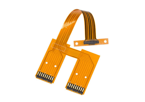
Correct pattern orientation and placement
In Flex PCB design, achieving the correct pattern orientation and placement is not just about aesthetics or organization; it directly affects the functionality, efficiency, and longevity of the PCB. Pattern orientation refers to how conductive patterns are placed with respect to the direction of the bend. Ensuring that circuits run perpendicular to the bend axis helps prevent mechanical stresses which might lead to circuit breakage over time. Placement of these circuits, on the other hand, involves tactically distributing components and circuit patterns on the board in a way in that respects bend areas, minimizes strain and meets design rules related to copper thickness, hole size, spacing, etc. Negligence in pattern orientation and placement can lead to suboptimal performance, signal integrity issues, or premature failure of the PCB. Thus, understanding and applying this concept ensures a more reliable and efficient Flex PCB design necessary for demanding technological applications.
Importance of understanding stiffeners
Stiffeners serve an indispensable role in Flex PCB design, offering mechanical support to cognate components during assembly and end-product use. These components can range from connectors, which require structural support to endure constant interconnect stress, to surface-mounted devices that necessitate rigid areas to avoid bending-induced damage. Stiffeners, typically made from materials like FR4 or Polyimide, are strategically used in Flex PCB designs to enhance rigidity in critical areas without compromising the board’s flexibility where required. By comprehending the importance and function of stiffeners, designers can aptly utilize them to increase the overall structural robustness of the PCB, protect components from mechanical strain, and ensure the reliable functionality of the flexible printed circuit board. Simply put, understanding stiffeners is crucial for ensuring the durability, reliability, and longevity of a Flex PCB design, particularly in mechanically demanding applications.
Function of stiffeners
A stiffener’s function in a Flex PCB design extends beyond what the name might suggest. Stiffeners offer targeted mechanical reinforcement to specific areas of the flexible circuit, allowing the protection of certain components and regions from undue mechanical stress, thermal loads, and wear-and-tear. Essentially, stiffeners work by providing rigidity to regions that house mounted components or areas that connect to other parts of the device, thereby preventing potential damage caused by excessive bending or flexing. They also assist in maintaining the flatness of a flex circuit during high temperature processing, making component soldering void of distortions. Moreover, stiffeners often provide thickness in regions where thickness matching is necessary for connectors. By comprehending the multifaceted functionality of stiffeners in Flex PCB design, one can skillfully integrate them into their designs to secure superior circuit robustness and endurance, thereby optimizing the product’s overall performance and lifespan.
The role of stiffeners in Flex PCB design
The role of stiffeners in Flex PCB design is incredibly significant and multifunctional. They serve as customized enhancements, offering mechanical support and effectively adding localized rigidity to flex circuits, particularly in areas housing surface-mounted devices or experiencing constant interconnect stress. Stiffeners ensure these essential elements remain stable and withstand potential mechanical strain or thermal impacts from manufacturing and operation. Furthermore, they facilitate compatibility with connectors and prevent distortion during high-temperature processing, like soldering. Stiffeners also help maintain circuit flatness, thereby reducing the chances of circuit breakage or fracturing on bending. They can even be used to help manage the CTE mismatch between the flexible circuit material and the components. Hence, understanding and correctly implementing the role of stiffeners is key to delivering a durable, efficient, and high-performance Flex PCB design that stands up to the demands of varying industrial applications.
Understanding Via-in Pad technology
Via-in Pad technology is an innovative method in PCB design that involves placing the vias, or passage points, directly beneath the components’ footprints or pads. This unique strategy effectively aids in achieving higher density circuit layouts, making it highly advantageous for Flex PCB designs, which often need to meet stringent space and weight constraints. Via-in Pad technology not only allows for miniaturization by providing room to place more components but also improves thermal management and enhances signal integrity in high-speed designs. However, it is crucial to manage potential challenges associated with the technique, such as potential issues with soldering due to the via’s capacity to wick away solder paste. Therefore, understanding Via-in Pad technology, along with its proper implementation and potential pitfalls, emerges as a crucial knowledge point for designers seeking to optimize their Flex PCB designs.
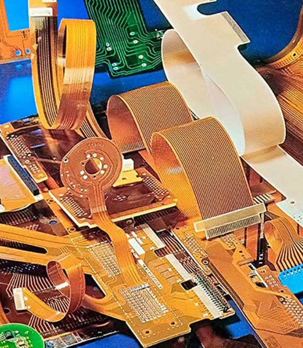
Importance of specialized materials for Flex PCBs
Material selection plays a pivotal role in Flex PCB design and can greatly influence the performance, flexibility, and reliability of the end product. The specialized materials used in Flex PCBs, such as polyimide, provide the bendability that distinguishes flex circuits from their rigid counterparts. These materials are designed to withstand tens of thousands of flexing cycles, maintain their insulating properties under high operating temperatures, and offer excellent chemical resistance. For the conductive layer, copper is typically favored due to its outstanding conductive properties and fatigue resistance. Choosing specialized adhesives that bind these layers together again matters immensely, as it needs to maintain cohesion and reliability through varying conditions of heat, moisture, and continuous flexing. In essence, understanding and selecting the optimal specialized materials for Flex PCBs are vital considerations in achieving a successful, efficient, and durable design. An informed material choice can enhance product longevity, operational efficiency, and ultimately influence the device’s market success.
Emphasizing on proper strain relief
In a Flex PCB design, incorporating proper strain relief is as fundamental as any other design aspect, if not more. Strain relief elements are designed to prolong the lifespan of the PCB by mitigating potential physical stresses caused by constant flexing, twisting or bending action. In its most basic form, strain relief can be built into the design by incorporating smooth, curved transition areas instead of abrupt changes in direction or width. This aids in distributing the mechanical stress over larger areas, thereby minimizing the risk of concentrated stress points leading to failures in the circuit traces. In other instances, strain relief can take the form of additional stiffeners or specifically designed flex regions. A well-thought strain relief design can prevent potential cracking of conductive paths, delamination, and other deformities associated with mechanical stress. Therefore, understanding and emphasizing proper strain relief in your Flex PCB design is a critical factor in enhancing the reliability, functional longevity, and overall performance of the product.
Explanation of strain relief
Strain relief is an essential concept in Flex PCB design, devised to alleviate the impact of physical stresses on the circuit board through strategic design measures. If you’ve ever wondered how a flexible PCB withstands continuous bending, flexing, and wiggling without showing signs of strain, the credit goes largely to effective strain relief. With a role centered around dispersing mechanical stress across an extended area of the board, strain relief strategies prevent any localized build-up of strain that could develop into circuit breakage or failure. This clever balancing of forces is often achieved by introducing certain design elements such as curved bend regions, reinforcing layers in areas of high strain, or maintaining a gradual transition at parts where the board’s thickness changes. By offering a well-thought-out strain relief design, you are essentially increasing the survivability and durability of your Flex PCB in its environment.
How strain relief impacts Flex PCB design
The inclusion of effective strain relief measures in a Flex PCB design can be a game-changer, significantly improving the design’s durability, functionality, and ultimately, its overall lifespan. Strain relief methods, by preventing strain concentration and distributing mechanical stresses evenly, play a substantial role in guarding the flexible circuits from potential physical damages arising from incessant bending, flexing or any other form of mechanical stress that flex circuits are typically subjected to. By doing so, strain relief ensures the design remains mechanically robust and reliable for an extended period, making it particularly crucial for applications where the boards are expected to flex regularly. Furthermore, strain relief impacts the efficiency of the PCB by preventing potential disruptions in the circuit’s conductive paths caused by mechanical strain. Therefore, understanding the profound impact of strain relief on a flexible PCB’s design can be the guiding factor towards creating a sturdy, resilient, and high-performing Flex PCB design.
Consistency in design rules
Consistency in design rules serves as one of the foundational elements in delivering a successful Flex PCB design. These rules, encompassing guidelines related to material selection, strain relief, pattern placement and orientation, Via-in Pad technology, and more, act as a roadmap to ensure the design’s effectiveness, manufacturability, and durability. Ensuring adherence to these rules at every design stage helps eradicate potential design and manufacturing issues, thereby guaranteeing a smoother path from conception to realization. Moreover, a consistent application of design rules enhances the predictability of the design’s performance and its in-service reliability, ultimately leading to superior product quality. So, an intricate understanding and steadfast application of these set design rules is essential to reap the benefits of a more reliable, robust, and high-performing Flex PCB design.
Conclusion
As the complexity and demand of electronic designs amplify in today’s swiftly evolving technological world, understanding the key elements of Flex PCB design becomes a cardinal requirement. This article, discussing the 7 Must-Knows for Your Flex PCB Design, underscores the importance of considering factors such as the tight bend radius, pattern orientation and placement, significance of stiffeners, the use of Via-in Pad technology, careful selection of specialized materials, proper strain relief, and adherence to consistent design rules. By gaining a thorough understanding of these fundamental aspects, both novice and experienced designers can navigate the intricate course of Flex PCB design with greater confidence and precision. As we strive to build electronic devices that are smaller, smarter, and more efficient, mastering these critical keys to Flex PCB design could undoubtedly pave the way to transforming concepts into successful and reliable products.