PCB (Printed Circuit Board) works by laying conductive copper foil on an insulating substrate to form an electrical connection between electronic components.PCB’s main function is to provide support for electronic components and electrical connections to simplify the assembly and welding of electronic equipment, reduce wiring workload, reduce labor intensity, while reducing the size of electronic equipment, reduce production costs and improve the quality and reliability of equipment. Labor intensity, while reducing the size of electronic equipment, reduce production costs, improve the quality and reliability of equipment.
Table of Contents
Composition of PCB
PCB is mainly composed of the following parts:
Substrate: usually made of glass fiber or epoxy resin, providing mechanical support and insulation.
Conductive layer: made of copper foil, responsible for transmitting current and signals.
Soldermask layer: protects the copper foil of the circuit board from oxidation and prevents short circuits.
Character layer: Marks the location of components on the circuit board for easy assembly and maintenance.
Composition of circuit board layers
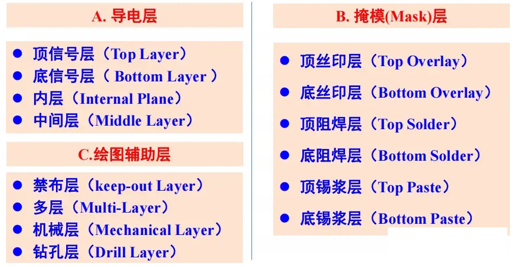
Circuit boards include many types of working layers, such as signal layers, protective layers, screen printing layer, internal layers, etc.
(1) shielding layer: mainly used to ensure that the circuit board does not need to be tin-plated places are not tin-plated, so as to ensure the reliability of the circuit board operation. Among them, TopPaste and BottomPaste are respectively the top and bottom soldermask layer; TopSolder and BottomSolder are respectively the solder paste protection layer and the bottom of the solder paste protection layer.
(2) Signal layer: mainly used to place components or wiring, ProtelDXP usually contains 30 intermediate layers, i.e. MidLayer1~MidLayer30, the middle layer is used to lay out the signal lines, the top layer and the bottom layer are used to place components or copper.
(3) Silk-screen layer: It is mainly used to print the running number of components, production number, company name, etc. on the circuit board.
(4) Internal layer: mainly used as a signal wiring layer, ProtelDXP contains a total of 16 internal layers.
(5) Other layers: mainly includes 4 types of layers.
DrillGuide (Drill Orientation Layer): Mainly used for drilling holes on the printed circuit board.
Keep-OutLayer (prohibit wiring layer): mainly used to draw the electrical border of the circuit board.
DrillDrawing: Mainly used to set the shape of the drilled holes.
Multi-Layer: Mainly used to set the multi-layer.
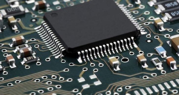
Circuit boards are mainly composed of pads, perforations, mounting holes, wires, components, connectors, SMT patches, filling, electrical boundaries, etc. The main functions of each component are as follows:
Solder pads: metal holes for welding component pins.
Through-hole: there are metal through-hole and non-metallic through-hole, of which the metal through-hole is used to connect the component pins between the layers.
Mounting holes: used to fix the circuit board.
Wires: Copper film used to connect the component pins of the electrical network.
Connectors: Used to connect components between circuit boards.
Filling: Copper laying for the ground network, which effectively reduces the impedance.
Electrical Boundary: Used to determine the dimensions of the circuit board, all components on the board can not exceed this boundary.
Types of PCBs
Based on the number of conductive layers, PCBs can be categorized as follows:
Single-sided board: only one side is a conductive layer, the other side is a non-conductive material, suitable for low-complexity circuits.
Double-sided board: both sides have a conductive layer, you can connect the two sides of the line through the over-hole, suitable for complex circuit design.
Multilayer boards: have more than three conductive graphic layers, connected by internal wires, suitable for highly integrated circuits
What are the electronic components above the PCB
Resistors: Resistors create electrical resistance to current. The most commonly used resistors are carbon-based resistors (commonly used for a variety of applications), metal film resistors (commonly used for precision circuits), and wirewound resistors (used in power circuits and amplifiers).
Capacitors: Capacitors are used to store energy in electronic devices. Series of capacitors are widely used in electronic products, including ceramic capacitors, electrolytic capacitors, and tantalum capacitors.
Inductors: Inductors store energy by generating a magnetic field. They help to power various devices, regulate voltage levels and suppress unwanted noise.
Potentiometers: Potentiometers regulate the amount of electricity flowing through them. They are commonly used to control the volume, tone and brightness of various devices.
Transformers: Transformers transfer energy between circuits, they help the electricity to move in different directions and change the voltage.
Diode: In a diode, current flows in only one direction. Diodes are usually made of silicon or germanium.
Transistors: Transistors are also known as “gatekeepers” because they regulate the power and current in a circuit. They are made of materials such as silicon or germanium. They come in many forms, including field effect transistors (FETs) and bipolar junction transistors (BJTs).
Silicon Controlled Rectifier (SCR): The SCR (called a thyristor) allows current to flow in one direction. It is adaptive and can be turned on and off at specific points in the circuit. Its main function is to control the power in a circuit.
Integrated Circuit: Many electrical components, such as transistors, resistors, capacitors, etc., are attached to a small silicon wafer to create an integrated circuit (IC). Engineers then combine them to create complex circuits that perform a variety of functions.
Oscillator: Quartz oscillators utilize the mechanical movement of a crystal to produce a precise frequency. They are an important part of GPS systems, watches, wristwatches, and other timekeeping devices.
Switches and Relays: Switches and relays can be used to evaluate the movement of electricity and the exact function of a device. A switch allows or prevents the flow of current in a circuit. It also acts as a bridge, thus connecting and disconnecting electrical channels.
Sensors: Sensors work by receiving various types of inputs (e.g. sound, pressure, temperature, heat, humidity sensors, position, vibration, etc.) and outputting them in the form of signals.
How Printed Circuit Boards Work
PCB Design Phase
Printed circuit boards require specialized design software to be carried out, where the designer places components, wiring paths and layers according to requirements, functionality and space availability.
Manufacturing Phase
The manufacturing process begins with the completion and refinement of the design process. A thin copper foil is used to cover both sides of the substrate to form a conductive layer. The copper layer is then removed by etching or printing, leaving the track and pad patterns needed to form the circuit. The next step is to drill holes at specific points on the PCB through which components and vias are routed to maintain electrical connections between the different layers. A layer of solder is then applied to the copper tracks and pads, leaving space for soldering components. A layer of solder is also usually applied to the end of the board to protect the exposed copper and provide strength to the board.
Adding Electronic Components
Once the PCB has been fabricated, electronic components need to be installed on it, which is generally accomplished in one of two ways.
Through-hole mounting (THT) technology, where components with leads are secured into pre-drilled holes in the board and the leads are soldered on opposite sides.
Surface Mount Technology (SMT), where components without leads are soldered directly to the printed circuit board.
Inter-component Relationships
The connection between the mounted components is made by means of conductive tracks on the printed circuit board. These tracks act as gateways for the free flow of electric current, thus forming the circuit.
Printed Circuit Board Testing
Once the components have been soldered to the board and the connections between them have been verified, the PCB undergoes rigorous and continuous testing to ensure proper operation. This includes continuity checks, signal integrity analysis and functional testing.
Integration
Once the functionality of a PCB has been successfully demonstrated, it can be used in the system or device for which it was designed. It can be connected to other PCBs or external devices to complete the entire system.
PCB Application Scenarios and Prospects
PCB is widely used in various electronic devices, from small electronic watches and calculators to large computers, communication equipment, military systems, etc. It is not only the support body of electronic components, but also a key component to realize the electrical connection between components. It is not only the support body of electronic components, but also the key component to realize the electrical connection between the components.PCB industry is one of the most important industries in the global electronic components sub-sector, and the market demand is very strong. With the development of emerging fields such as 5G, integrated circuits, new energy vehicles and digital economy, the PCB market outlook is very broad.Since 2016, the global PCB market value has continued to grow rapidly, and it is expected that by 2028, the global PCB production value will reach 90.413 billion U.S. dollars, with an estimated compound annual growth rate of 5.40% from 2023 to 2028 . In addition, the manufacturing quality of PCB directly affects the reliability and competitiveness of electronic products, so its technology level and the continuous improvement of market demand provides a strong impetus for the development of the industry.