Get a Quote
OUR BLOG
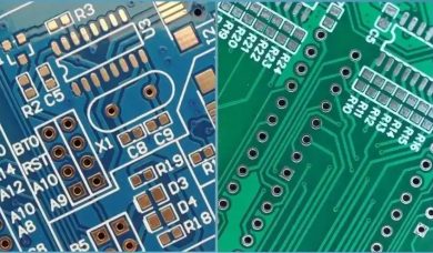
PCB surface treatment process, refers to the PCB board components, electrical connections on the artificial formation of a layer and the substrate's mechanical, physical and chemical properties of the surface layer, the core purpose is to ensure that the PCB has a good solderability and electrical properties.
15
Mar
Layers 1 Layers 2 Layers 4 Layers 6 Layers 8 Layers 10 Layers 12 Layers 14 Layers
Dimensions (mm)
Quantity 5 10 15 20 25 30 35 40 50 75 100 100+
Thickness 0.4mm 0.6mm 0.8mm 1.0mm 1.2mm 1.6mm 2.0mm 2.4mm
Quantity
Number of Unique Parts
SMT Pads
Thru-Holes