In modern electronics manufacturing, SMT (Surface Mount Technology) has become the core process for PCB assembly. This article delves into all aspects of SMT technology, including its working principles, complete workflow, common issues and solutions, as well as practical tips. Whether you’re new to electronics manufacturing or a professional looking to optimize production lines, you’ll find valuable insights here.
Table of Contents
What is SMT Technology?
SMT (Surface Mount Technology) is an advanced process that directly mounts electronic components onto the surface of a PCB (Printed Circuit Board), achieving reliable electrical connections through reflow soldering. Compared to traditional through-hole technology (DIP), SMT eliminates the need for drilling numerous holes in the PCB—components simply “sit” on the pads, greatly simplifying the manufacturing process.
Why is this technology so important? There are three main reasons:
- Cost Efficiency: Fewer drilled holes mean significantly lower processing costs, making it ideal for mass production.
- Space Savings: SMT components are much smaller than traditional ones, enabling thinner and lighter electronic devices.
- Performance Boost: Shorter leads result in lower parasitic inductance and capacitance, improving circuit performance.
Imagine modern smartphones packed with components—without SMT, they might still be as bulky as the “brick phones” of the past. That’s the transformative power of SMT in the electronics industry.
Step-by-Step Breakdown of the SMT Process
Pre-Production: The Foundation of Success
Circuit Design is the starting point of SMT. A well-thought-out design must consider:
- Optimal component placement (keeping high-frequency components away from interference sources)
- Trace optimization (avoiding sharp angles, considering current-carrying capacity)
- Pad design (size and shape matching the components)
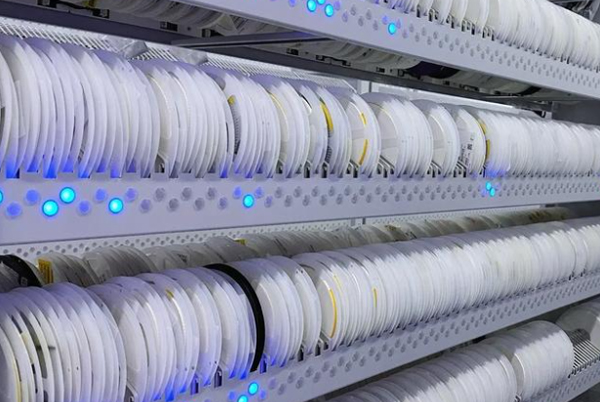
Component and Equipment Preparation is equally crucial:
- Verify component specifications against the BOM (Bill of Materials)
- Calibrate the placement machine accuracy (typically within ±0.05mm)
- Check the temperature uniformity of the reflow oven
I once saw a factory skip the solder paste thawing step, using it straight from refrigeration, which caused an entire batch of products to suffer from cold solder joints, costing them dearly. Pre-production prep is no place for shortcuts!
Solder Paste Printing: The Art of Precision
Stencil Fabrication comes first:
- Laser-cut stainless steel sheets with openings matching the PCB pads 1:1
- Choose thickness (typically 0.1–0.15mm, adjusted based on component size)
Solder Paste Handling Tips:
- Thaw for at least 4 hours (if refrigerated)
- Stir to a smooth, “peanut butter” consistency
- Control the printing environment (23±3°C, humidity <60%)
Print Quality Checks:
- Inspect the paste shape under a magnifier for completeness
- Measure thickness (usually 80–90% of stencil thickness)
- Look for issues like tailing, gaps, or bridging
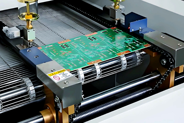
Component Placement: Balancing Speed and Accuracy
Modern pick-and-place machines are astonishing:
- High-speed machines can place over 150,000 components per hour
- Multiple nozzles working simultaneously boost efficiency
- Vision systems ensure precise alignment (±0.025mm)
Programming Tips:
- Optimize the placement sequence to minimize travel distance
- Place larger components last to avoid interference
- Set special parameters for unique components (e.g., QFN)
Pro tip: Clean nozzles regularly—I’ve seen a tiny 0.1mm solder paste residue cause an entire batch of misaligned components.
Reflow Soldering: The Dance of Heat
Temperature Profile Setup is key:
- Preheat zone (1–3°C/sec, up to 150–180°C)
- Soak zone (60–120 sec for even board heating)
- Reflow zone (peak temperature 20–30°C above solder melting point)
- Cooling zone (controlled at ≤4°C/sec)
Common Pitfalls:
- Too-rapid heating can cause thermal stress damage
- Insufficient peak temperature leads to cold solder joints
- Excessive heat may damage components or the PCB
Inspection & Testing: Guardians of Quality
AOI (Automated Optical Inspection) Essentials:
- Set appropriate detection parameters (e.g., solder joint brightness thresholds)
- Regularly calibrate the camera system
- Build a library of typical defect samples
Functional Testing Strategies:
- Verify modules step by step
- Test under boundary conditions (e.g., voltage fluctuations)
- Use Environmental Stress Screening (ESS) to enhance reliability

SMT vs. SMD: Key Differences Explained
Many beginners confuse these two terms:
SMD (Surface Mount Device) refers to electronic components designed specifically for surface mounting. They feature:
- No long leads, only flat contact surfaces
- Examples: resistors, capacitors (0805, 0603 packages), QFP/BGA ICs, small inductors, diodes
SMT (Surface Mount Technology) is the entire process of mounting SMD components onto PCBs, including:
- Printing, placement, and soldering equipment
- Process flow control
- Quality inspection standards
In short, SMD is the “what,” and SMT is the “how.” Think of bricks (SMD) vs. bricklaying techniques (SMT).
Top 5 Common SMT Issues & Solutions
Issue 1: Why is the solder paste print irregular?
Possible Causes:
- Residual paste under the stencil
- Uneven or worn squeegee pressure
- Uneven PCB support
- Incorrect solder paste viscosity
Solutions:
- Clean the stencil bottom every 5–10 prints
- Check the squeegee for damage; set pressure to 5–8 kg/cm²
- Adjust support pins to ensure PCB flatness
- Test paste viscosity (target: 800–1200 kcps)
Issue 2: Components shift after placement—what to do?
Possible Causes:
- Weak nozzle vacuum
- Incorrect component thickness setting
- PCB misalignment
- Improper placement height
Solutions:
- Check for vacuum leaks; clean or replace nozzles
- Remeasure component thickness and update the database
- Recalibrate PCB fiducial marks
- Adjust placement height (typically 0.1mm below component height)
Issue 3: Solder balls after reflow—why?
Possible Causes:
- Excessive solder paste
- Too-rapid temperature ramp-up
- Poor stencil aperture design
- High humidity
Solutions:
- Reduce stencil aperture size (e.g., 10% inward step)
- Adjust preheat ramp rate to 1–3°C/sec
- Use trapezoidal or home-shaped apertures
- Maintain workshop humidity at 40–60% RH
Issue 4: How to troubleshoot BGA voiding?
Possible Causes:
- Poor solder ball coplanarity
- Moisture in PCB/BGA
- Mismatched temperature profile
- PCB warping
Solutions:
- Use an X-ray to check the solder joint fusion
- Bake moisture-sensitive components (125°C, 12–24 hrs)
- Extend the time above the liquidus in the reflow profile
- Add support points to minimize PCB warpage
Issue 5: How to reduce QFN soldering defects?
Possible Causes:
- Insufficient solder on the thermal pad
- Bridging on perimeter pads
- Misalignment
Solutions:
- Set stencil aperture ratio at 60–70% for the center pad
- Use the “cross” pattern for perimeter pads
- Add optical alignment checks
- Increase stencil thickness slightly (e.g., 0.15mm)
Advanced Tips & Industry Trends
Handling Special Components
Ultra-Small Components (01005 or smaller):
- Use high-precision electroformed stencils
- Reduce squeegee angle (45–55°)
- Increase post-placement inspection frequency
Odd-Form Components:
- Custom nozzles
- Dedicated vision parameters
- Possible secondary reflow process
Lead-Free Process Considerations
With rising environmental regulations, lead-free soldering is becoming standard:
- Higher melting point (217°C vs. 183°C for leaded)
- Poorer wetting—optimize stencil design
- Narrower process window—tighter temperature control
Smart Manufacturing in SMT
Cutting-edge trends include:
- 3D SPI (Solder Paste Inspection) real-time feedback
- Digital twin simulation for optimization
- AI-driven defect recognition
- Predictive equipment maintenance
Practical Advice & Recommended Resources
Documentation Best Practices:
- Record optimal parameters for each product
- Archive defect images and solutions
- Regularly update operating procedures
Key Training Areas:
- Equipment maintenance basics
- Quick troubleshooting skills
- ESD protection awareness
Recommended Tools:
- Magnifier/microscope (30–100x)
- Temperature profiler
- Solder paste viscometer
Industry Resources:
- IPC-A-610 (Acceptability of Electronic Assemblies)
- SMTA (Surface Mount Technology Association) seminars
- Application notes from leading equipment vendors
Final Thoughts
As the backbone of modern electronics manufacturing, SMT technology’s importance cannot be overstated. Mastering key process points—from solder paste printing to reflow soldering—and understanding root causes of common issues can significantly enhance production quality and efficiency. With components shrinking and process demands rising, continuous learning and hands-on optimization are essential for every SMT engineer.
Remember: Excellent SMT processes = scientific methods + rigorous discipline + accumulated experience. May this guide serve as a valuable reference in your work, and feel free to share your insights and experiences!