SMT placement, or Surface Mounted Technology (SMT), covers the assembly and placement technology of printed circuit boards and has become one of the most widely adopted advanced processes in the electronic assembly industry. In the electronic equipment manufacturing industry, SMT is a key production process, and its efficiency and accuracy in improving product quality and reducing costs is of great significance. The diversity and complexity of electronic products, so that each product requires a specific SMT placement process, as electronic equipment industry practitioners, you need to have a deep understanding of the SMT process flow, to better serve customers, to solve customer concerns.
SMT basic process overview
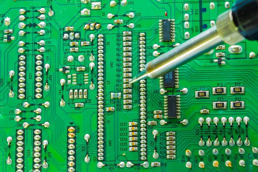
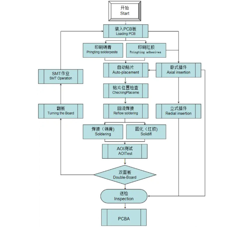
SMT process flow mainly includes screen printing (or dispensing), mounting, curing (for the dispensing process), reflow soldering, cleaning, testing, and rework steps.
SMT simple process: utilizing silk screen printing the solder paste is printed accurately to the PCB pads, and then glue drops to a specific location on the PCB to fix the components, and then through the mounting of the surface assembly components are accurately placed in the preset position of the PCB, and then through the curing oven to make the patch adhesive melting, thus ensuring that the components and PCB board firmly bonded, and then through the reflow oven to melt the solder paste to achieve the Components and PCB board firmly connected, after completing these steps, the need to remove the assembly process of harmful welding residues, such as flux, etc., these steps are interlocked, together constitute the core process of SMT production, each step needs to be standardized and accurate. Finally, the detection link, the use of a variety of equipment such as magnifying glasses, microscopes, online testers, etc. on the assembly of the completed PCB board for comprehensive quality testing to ensure product reliability and performance.
Below is an introduction to several common SMT assembly processes
1、Single-side assembly process
Process flow
Incoming material inspection → silkscreen solder paste (or point patch adhesive) → patch → drying (curing, for the dispensing process) → reflow soldering → cleaning → testing → rework
Application Scenario
Single-sided assembly process only one side of the SMD devices needs to be soldered. It is suitable for products with a small number of components and low circuit complexity. The advantage is that the process is simple and low cost, but the space utilization rate is low, for high-density, high-performance products may not meet the demand.
2、Double-sided assembly process
Process Flow
The double-sided assembly process is divided into A-side and B-side of the two main steps, usually dealing with one side, and then turning the plate to deal with the other side.
Side A processing flow: incoming material detection → silkscreen solder paste (or spot patch adhesive) → patch → drying (curing) → reflow soldering → cleaning → Flipboard.
Side B processing flow: silkscreen solder paste (or dot patch adhesive) → patch → drying (curing) → reflow soldering → cleaning → testing → repair.
Note
Side A are SMD components, when dealing with side B, need to ensure that the components of side A are not affected. The double-sided assembly process makes full use of the PCB space, suitable for high-density, high-performance products. However, the complexity of the process is higher and the cost increases accordingly.
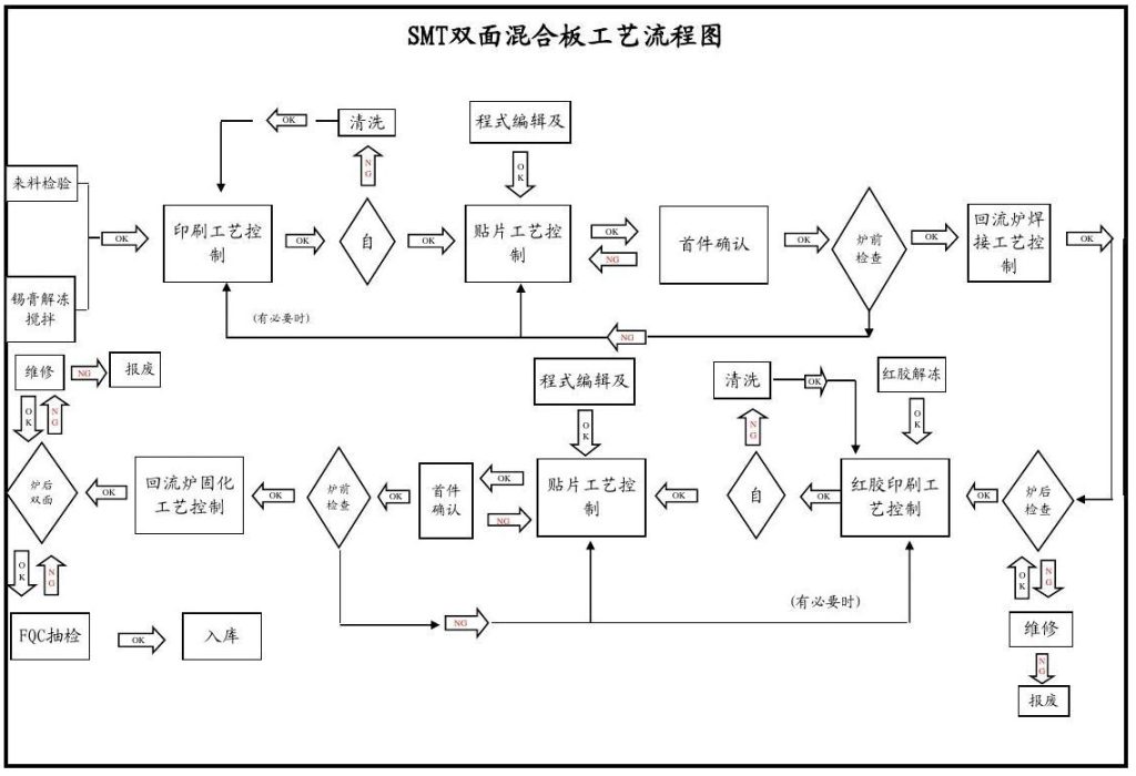
3、Single-double-side mixed assembly process
Single and double-sided mixed assembly process combines SMT chip components and through-hole inserted components, further improving the flexibility of PCB layout and functional diversity.
A-side mixed assembly, B-side mounting
A-side processing flow: incoming material inspection → inserted components (through-hole components) → wave soldering → flip-chip.
B-side processing flow: silkscreen solder paste (or dot patch adhesive) → patch → drying (curing) → reflow soldering → cleaning → testing → repair.
B-side mixing, A-side mounting
B-side processing flow: incoming material testing → insert (through-hole components) → wave soldering → flap.
A-side processing flow: silkscreen solder paste (or dot patch adhesive) → patch → drying (curing) → reflow soldering → cleaning → testing → repair.
Precautions
The mixed assembly process needs to strictly control the order of insertion and placement to avoid mutual interference. The temperature and time parameters of wave soldering and reflow soldering need to be optimized according to the characteristics of the components.
SMT process flow of single and double-sided assembly and single and double-sided mixed assembly process have their own characteristics, suitable for different application scenarios, can realize high-density assembly, high degree of automation, excellent electrical performance, improve production efficiency, reduce costs and improve quality, adaptability, environmental protection, flexibility and innovation potential. It also offers flexibility and innovation potential.