Table of Contents
Printed Circuit Board (PCB) Overview
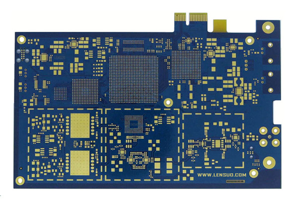
A Printed Circuit Board (PCB) is a fundamental component in electronics that provides mechanical support and electrical connections for electronic components. Once assembled, it forms a complete functional circuit. PCBs can be designed as single-layer, double-layer, or multi-layer boards with printed conductive traces, pads, and insulating materials.
Key Components of a PCB:
- Substrate (Base Material): Typically made of FR4 fiberglass, providing mechanical strength and insulation.
- Copper Layer: Conductive traces etched onto the substrate to form electrical connections.
- Solder Mask: A protective coating that prevents short circuits and oxidation.
- Silkscreen: Printed markings for component labeling and assembly instructions.
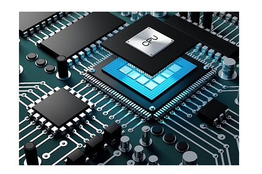
Printed Circuit Board Assembly (PCBA) Process
Printed Circuit Board Assembly (PCBA) refers to transforming a bare PCB into a functional circuit by mounting and soldering electronic components. This involves Surface Mount Technology (SMT) and Plated Through-Hole (PTH) techniques, followed by soldering, inspection, and testing.
Key PCBA Manufacturing Steps:
- Component Placement:
- SMT (Surface Mount Technology): Automated pick-and-place machines position tiny components (resistors, capacitors, ICs) onto the PCB.
- PTH (Plated Through-Hole): Traditional insertion of leaded components into drilled holes.
- Soldering:
- Reflow Soldering: Used for SMT components, where solder paste is melted in a controlled heating process.
- Wave Soldering: Primarily for through-hole components, where the PCB passes over a molten solder wave.
- Quality Control & Testing:
- AOI (Automated Optical Inspection): Detects assembly defects like misalignment or solder issues.
- X-ray Inspection: Checks hidden solder joints (e.g., BGA components).
- Functional Testing: Verifies electrical performance and reliability.
PCBA ensures proper electrical connections between components and circuits while guaranteeing the board functions as intended. As electronics evolve toward miniaturization and high-density designs, PCBA technology continues to advance to meet stringent manufacturing demands.
Core Differences Between PCB and PCBA
1. Fundamental Distinctions
Definition & Functionality
- PCB (Printed Circuit Board): Serves as the physical substrate for electrical connections, containing no active/passive components.
- PCBA (Printed Circuit Board Assembly): A fully functional module with all components mounted on the PCB.
Manufacturing Comparison
| Stage | PCB Fabrication | PCBA Assembly |
|---|---|---|
| Key Processes | Patterning, Etching, Drilling, Surface Finish | Solder Paste Printing, Pick-and-Place, Reflow Soldering |
| Critical Equipment | Exposure Systems, Etching Lines, Laser Drills | SMT Pick-and-Place Machines, Reflow Ovens, AOI Systems |
| Output | Bare Board (Non-functional) | Functional Electronic Module |
Cost Structure
PCB costs focus on substrate and patterning (30-50% of total), while PCBA costs are dominated by components (60-70%) and assembly precision.
2. Process Flow Deep Dive
PCB Core Processes
- Patterning: LDI exposure transfers Gerber files to copper-clad laminates
- Precision Etching: Differential etching achieves 3μm line width tolerance
- Interlayer Connections: Laser drilling + via filling (20:1 aspect ratio)
- Surface Finish: ENIG/OSP treatments prevent oxidation
PCBA Critical Stages
- Solder Paste Printing: Stencil thickness tolerance ±10μm
- Component Placement: 0402 component placement accuracy ≤50μm
- Soldering Processes:
- SMT: 8-zone reflow (peak temp 245±5°C)
- THT: Dual-wave soldering (3-5s contact time)
3. Application Evolution
PCB Advancements
- HDI Boards: Smartphone motherboards (≤40μm line/space)
- High-Frequency Materials: PTFE substrates for 5G (Dk≤3.0)
- Rigid-Flex: 3D routing for wearables
PCBA Innovations
- Automotive: SiP packaging in ADAS systems
- Medical: 0201 component arrays in biosensors
- Industry 4.0: AI accelerator-integrated smart modules
4. Industry Trends
Miniaturization
- SLP (Substrate-Like PCB) with 20μm lines
- Embedded components boost integration by 30%
Sustainable Manufacturing
- Halogen-free substrates to reach 65% adoption (2025 projection)
- ≥99.8% copper ion recovery in wastewater
Smart Inspection
- 3D SPI at 15cm²/s scan speed
- AI visual defect detection (99.95% accuracy)
5. Supply Chain Considerations
- Design Collaboration: DFM analysis during schematic phase
- Capacity Planning: Separate production lines for HDI (≥16L) and standard PCBs
- Certifications: Automotive requires IPC-6012 + IATF 16949 compliance
6. Technology Selection Guide
- Consumer Electronics: 4-6 layer HDI with 01005 components
- Industrial Control: 2oz copper + conformal coating
- High-Frequency Apps: Rogers RO4350B substrate